Hacking a Sega Whitestar Pinball
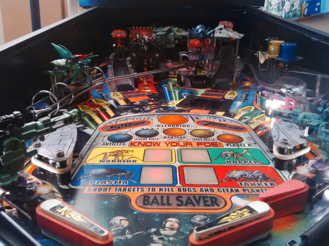
Sega Starship Troopers Pinball Overview
The Sega Starship Troopers Pinball is fairly representative of the
WhiteStar Board System used in several Sega pinball games and
Stern Pinball. This hardware architecture was firstly designed in 1995 for
the Apollo 13 game with the objective to be convenient and extensible in
order to be reusable for other playfields. This way, Sega could exploit a
large number of licenses without having to design new control circuits for each
machine.
This architecture is based on three Motorola 68B09E clocked at 2MHz and used
as main CPU, display controller and sound controller. The two last are mainly
dedicated to monitor application-specific processors: for instance, the 6809
used on the display board is charged to interface a 68B45 CRT controller to
the main CPU. The sound processing is handled by a BSMT2000, a custom
masked-rom version of the TI TMS320C15 DSP.
Sega used this system for 16 other games including GoldenEye, Star Wars and Starship Troopers.
Playfield’s wiring
The playfield wiring is quite simple: all switches are disposed in a matrix grid. This method provides a simple way to handle a high number of I/O with a reasonable number of connectors. So, in order to read the switches state, the CPU has to scan each raw of the matrix by grounding it and watching in which column the current is flowing.
A similar circuit is used to control playfield lamps: each raw has to be scanned by grounding it and applying voltage on the column connector according to lamps that have to be switched on the selected raw.
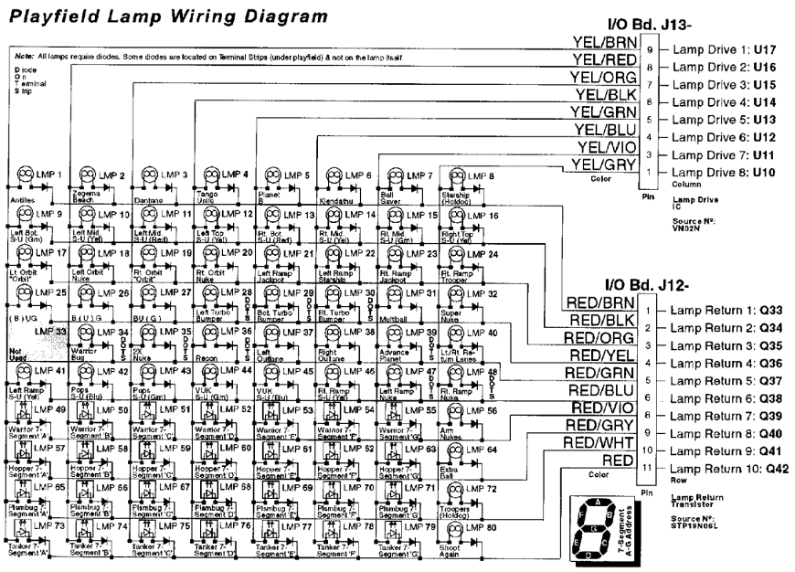
It’s truly easy to control a high number of lamps with this layout. The following code switches on the lamp 31 (multiball).
lda   #$8
sta   LAMP_ROW  ;; Ground selected row
clra
sta   LAMP_AUX  ;; Clear auxiliary rows
lda   #$40
sta   LAMP_COL  ;; Drive selected column
Although playfield switches are handled by the matrix grid, some frequently used buttons are connected to a dedicated connector. This allows the CPU to directly address this input without having to scan the entire input matrix. These switches are user buttons and End-Of-Stroke.
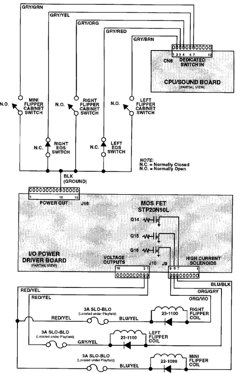
The E.O.S switch prevents foldback when the player has the flipper energized to capture balls. When the Game CPU detects that this switch is open, it stabilizes the position of the selected flip by reducing the pulse applied to the coil.
The Backbox
The Backbox contains all the electronic circuits controlling playfield’s behaviour. We will focus on this very part throughout the article.
CPU/Sound Board
The main board contains the Game CPU and the Sound circuit. The switches are directly connected to this board so that it is really simple for the CPU to fetch their values.
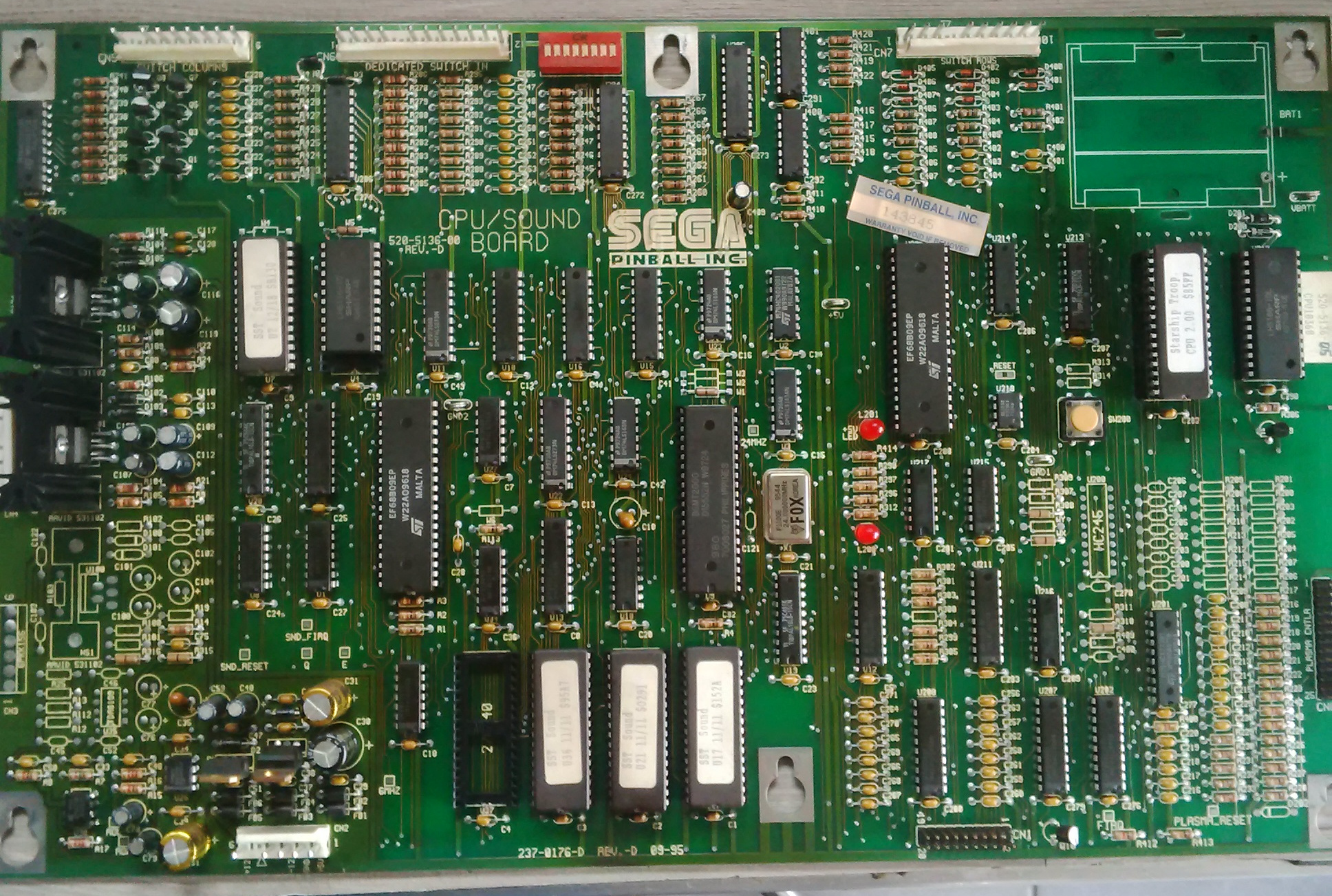
One of the main problems of this board is the battery location. Populated with a 3xAA battery holder to keep the RAM content alive, alkaline batteries are located on top of the CPU, ROM and RAM chip, which is critical when they will start to leak on this components. Before I started playing with this machine, I spend hours restoring and cleaning the PCB because of the corrosive leaking. To avoid deterioration, relocating this battery could be a smart idea.
Display Controller Board
Like many pinball machines from the 90s, the backbox is equipped with an old school dot matrix display.
As the CPU Board, it is based on a Motorola 68B09E with a dedicated 512MB
UVPROM which contains the dot matrix display driver code and images that can be
displayed on it. It communicates with the main board via a specific protocol.
To interface the raster display, the board uses a Motorola 68B45 (68B45 CRTC
for “cathode ray tube controller”). Although this chip was primarily
designed to control the CRT display, it can also be used to generate correctly
timed signal for a raster dot matrix display like in this case.
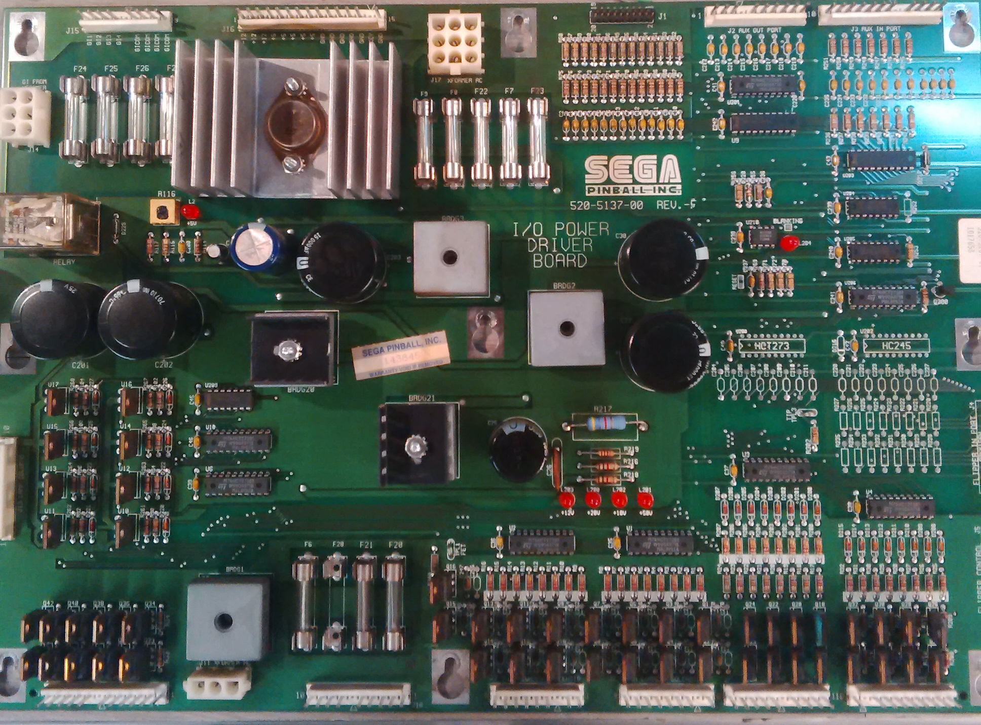
I/O Power Driver Board
The IO Power Driver Board is an interface between the low current logic circuit and the high current playfield circuit.
The first part of this circuit consists of converting the alternative current provided by the transformer into exploitable direct current thanks to 5 bridges rectifiers.
The only electromagnetic relay is dedicated to the general illumination and is not controllable via the main CPU. The rest is driven by MOSFET power transistors which are designed to be able to handle high current in order to power playfield coils. Moreover, fuses are placed before each bridges rectifiers in order to easily help identifying where the problem comes from in case of failure.
Upgrading the firmware
The title screen displayed in the dot matrix plasma display indicates that
the firmware’s version is 2.00. However, an up-to-date image of this ROM
exists in Internet Pinball Database
which seems to be on version 2.01 according to the ascii string located at
offset $66D7. Let’s try to upgrade the pinball!
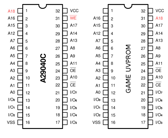
An almost suitable flash memory to replace the original UVPROM is the
A29040C. The only mismatches on the pinout are the A18 and WE pins. This
is a minor problem since I fixed the PCB to match the A29040C layout.
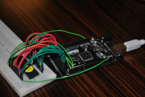
Burning the A29040C with the new firmware requires a flash memory programmer.
I decided to craft one with an Arduino mega 1280 based on an AVR Atmega 1280
microcontroller. The large number of IO of this chip is essential to complete
the programming protocol of the A29040C.
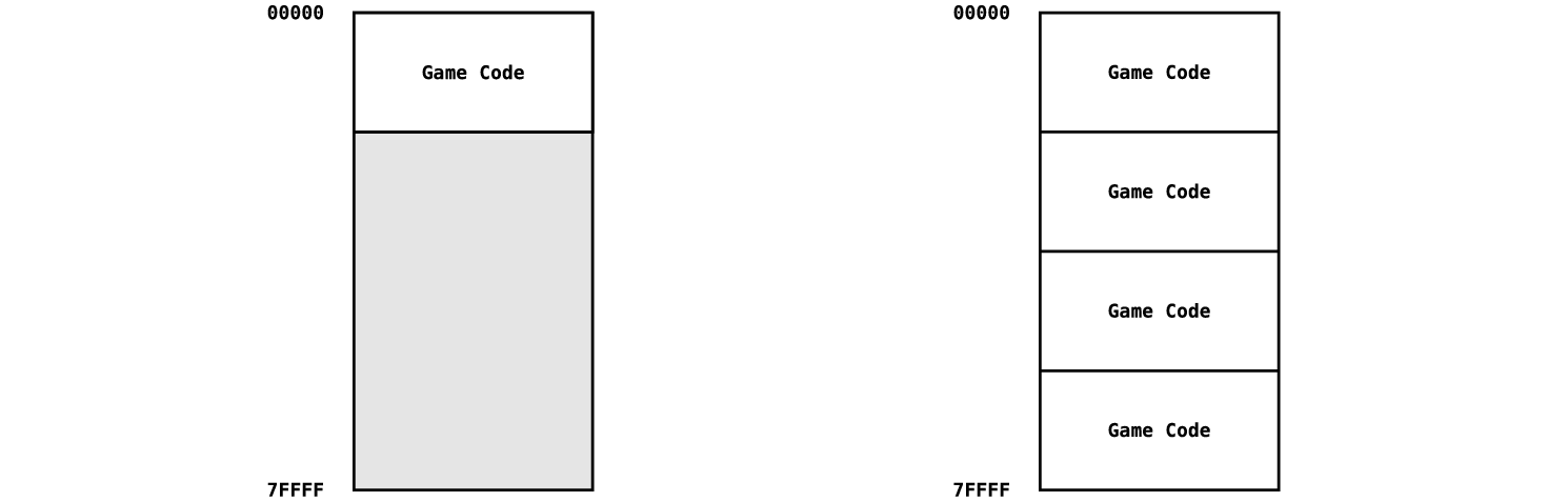
After successfully programming the flash memory, I was pretty disappointed when I noticed that the new ROM chip was still not working.
I thought that this UVPROM was able to store 512KB of data, just like
A29040C. It took me a while to realise that the game is a 128KB ROM although
the chip is designed to be connected to a 19 bit address bus. This means that
the game’s ROM simply ignores the value of A17 and A18 signals, which means
that the game code is mirrored 4 times in the whole ROM address space.
Building a custom ROM
Now that we are able to substitute the original ROM with a custom flash memory, let’s try to run our own code on this machine.
The first thing that we have to do in this case is to determine where the CPU
will fetch its first instruction after a reset.
According to the6809 datasheet, the interrupt vector table (which contents
the address of the reset event handler) is located at 0xFFFE. However, this
offset refers to the CPU address space, not that of the ROM chip. So, after a
reset, which part of this memory is mapped at 0xFFFE?
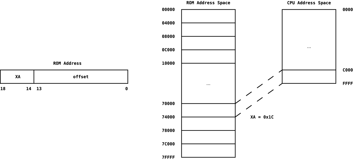
To answer this, it’s essential to follow the address bus of the UVPROM. We then
easily see that bits 14 to 18 of this bus are connected to 5-bit register
(U211) while bits 13 to 0 are directly bound to CPU address bus.
This is a typical configuration to implement a bank system since the CPU
address space is too narrow to map the entire ROM. That’s why only one part of
it (also called a bank) is mapped at a given time.
The mapped bank is chosen by the U211 register, called XA, and can be
easily wrote by the CPU when a bank switching is needed.
Finding address space
On this kind of device, it’s always painful to debug the code running directly on the board. The only way to achieve it here is to trigger some visual element of the playfield in order to get a basic tracing of the execution flow.
As there is no IO port on the 6809, all devices are memory-mapped. The
question now is: where are they located?
First, let’s focus on the address decoding circuit of the IO Board.
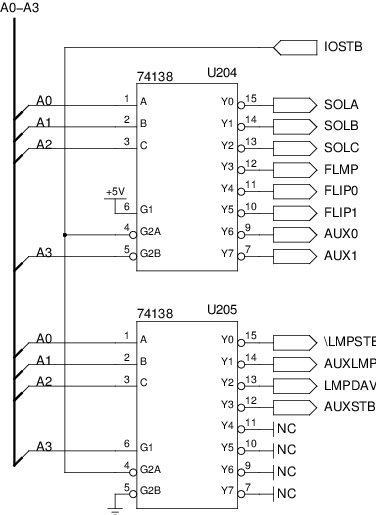
In order to simplify cascading, the 74138 multiplexer generates output only
if the Boolean expression G1 && !G2A && !G2B is true. So, in this circuit,
U204 covers IO addresses from 0x0 to 0x7 and U205 handles from 0x8 to
0xF.
As we can see on this schematic, the question is: where does the IOSTB signal
come from?
Following the wire, we can see that this control signal is generated by the CPU Board. It actually acts as a chip select: it means that this signal is used to indicates to the IO Board that we are addressing it.
To be more precise, the IOSTB is driven by the U213 chip, a PAL16L8
(Programmable Array Logic). This kind of integrated circuit is used to
implement combinatoric logic expressions. This is widely used for address
decoding.
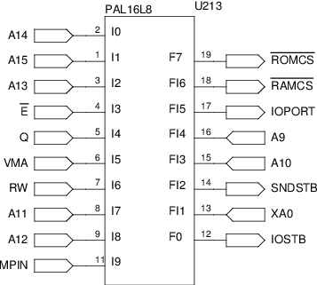
Dumping the logical expression programmed on this chip is essential to
determine the actual CPU address space. One way to do it is to basically
test all possible inputs and watch how outputs evolves according to input
values. However, some of the PAL16L8 pins can be considered as inputs as well
as outputs. In this case, we can guess that XA0, A9 and A10 are used as
input pins according to the rest of the circuit.
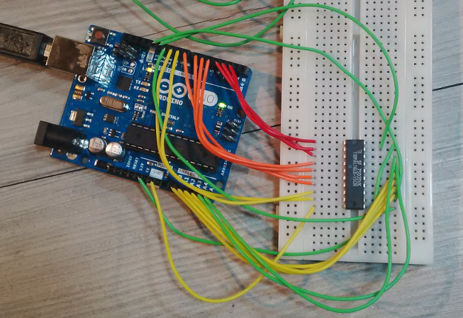
I desoldered the PAL, in order to prevent undesired side effect on the rest of the circuit, and used a simple Arduino Uno to generate the truth tables of all outputs.
Now, let’s extract irreducible logical expressions from the recorded truth tables. As a matter of fact, these truth tables are significantly too large to apply the well-known Karnaugh map method to simplify the extended logical expression. This problem can be solved by using the electruth python module. It fully implements the Quine-McCluskey method which is perfectly suitable in this situation.
After a few hours of computation, I got these expressions, which are truly helpful in the address space determination process:
~ROMCS = A15 || A14
~RAMCS = !A15 && !A14 && !A13 && (!A12 || !A11 || !A10 || !A9 || RW || MPIN)
IOPORT = !(!A15 && !A14 && A13 && !A12 && !A11 && !XA0)
IOSTB = !A15 && !A14 && A13 && !A11
Notice the MPIN input which is a signal generated by the cabinet door when
it’s open. So, the PAL restricts the access to a small part of the RAM when
the coin door is closed. This section is actually used to store game settings
that are only editable for maintenance purpose.
Here is the address space that I was finally able to discover according to the actual wiring:
0000-1FFF: RAM0000-1DFF: Read/Write Area1E00-1FFF: Write Protected Area
2000-27FF: IO (IOBOARD)2000: HIGH CURRENT SOLENOIDS A- bit 0 : Left Turbo Bumper
- bit 1 : Bottom Turbo Bumper
- bit 2 : Right Turbo Bumper
- bit 3 : Left Slingshot
- bit 4 : Right Singshot
- bit 5 : Mini Flipper
- bit 6 : Left Flipper
- bit 7 : Right Flipper
2001: HIGH CURRENT SOLENOIDS B- bit 0 : Trough Up-Kicker
- bit 1 : Auto Launch
- bit 2 : Vertical Up-Kicker
- bit 3 : Super Vertical Up-Kicker
- bit 4 : Left Magnet
- bit 5 : Right Magnet
- bit 6 : Brain Bug
- bit 7 : European Token Dispenser (not used)
2002: LOW CURRENT SOLENOIDS- bit 0 : Stepper Motor #1
- bit 1 : Stepper Motor #2
- bit 2 : Stepper Motor #3
- bit 3 : Stepper Motor #4
- bit 4 : not used
- bit 5 : not used
- bit 6 : Flash Brain Bug
- bit 7 : Option Coin Meter
2003: FLASH LAMPS DRIVERS- bit 0 : Flash Red
- bit 1 : Flash Yellow
- bit 2 : Flash Green
- bit 3 : Flash Blue
- bit 4 : Flash Multiball
- bit 5 : Flash Lt. Ramp
- bit 6 : Flash Rt. Ramp
- bit 7 : Flash Pops
2004: N/A2005: N/A2006: AUX. OUT PORT (not used)2007: AUX. IN PORT (not used)2008: LAMP RETURNS2009: AUX. LAMPS200A: LAMP DRIVERS
3000-37FF: IO (CPU/SOUND BOARD)3000: DEDICATED SWITCH IN- bit 0 : Left Flipper Button
- bit 1 : Left Flipper End-of-Stroke
- bit 2 : Right Flipper Button
- bit 3 : Right Flipper End-of-Stroke
- bit 4 : Mini Flipper Button
- bit 5 : Red Button
- bit 6 : Green Button
- bit 7 : Black Button
3100: DIP SWITCH3200: BANK SELECT3300: SWITCH MATRIX COLUMNS3400: SWITCH MATRIX ROWS3500: PLASMA IN3600: PLASMA OUT3700: PLASMA STATUS
4000-7FFF: ROM8000-BFFF: ROM (Mirror)C000-FFFF: ROM (Mirror)
Handling reset circuitry
In this kind of real-time application, where a huge number of unpredictable events have to be handled, the risk of race condition cannot be fully faded.
Although the software is designed to be able to face any situations, the hardware has to be prepared to a faulty program. One of the simplest and more robust method is to use a watchdog timer. This consists of an autonomous timer charged to trigger a reset signal to the system if it reaches its initial point. The main idea here is to force the circuitry to be stopped if it does not correctly respond in order to prevent any damage from uncontrolled behaviour.
In most cases, the timer has to be fed by the software running on the CPU. So, if we want to run our own code on that machine, it’s essential to implement as a subroutine the reset of the watchdog in order to stay alive.
In the Whitestar pinball, two distinct watchdogs have to be correctly handled.
The first one is located on the CPU/Sound Board and is directly connected to
the reset pin of the 6809. SEGA engineers chose to use a DS1232 chip
(U210) which integrates all the features that are commonly used to monitor a
CPU. So, in addition to a regular watchdog timer, this chip also provides a
power monitoring and an external override which is actually designed to allow
the use of a push button to force the CPU reset (SW200).
As the TOL pin of this chip is grounded, the DS1232 continually watches
the voltage applied on Vcc pin and triggers a reset signal if its value
is under 4.7V. From a software engineer point of view, the important pin in
that case is the strobe input (ST): it is used to reset the watchdog timer
when a falling edge is applied to it.
On the CPU/Sound Board, this pin is connected to either clock signal (generated
by U2) or BSEL signal according to the location of the jumper (Wx or Wy).
As Wx was jumpered on my board, we can assume that the configuration in which
Wy is fit was used during firmware development. So programmers were able to
test their code without having to mind about the watchdog reset: this was
automatically done by the clock signal. When the pinball was about to be
released, calls to the watchdog reset subroutine were injected in appropriate
parts of the firmware and the jumper was moved from Wy to Wx.
In my opinion, modifying the hardware by desoldering the jumper and resoldering
it on Wy is a little bit too easy to solve this kind of problem. So, let’s
try to handle the watchdog timer with a suitable software subroutine.
The BSEL signal is generated when writing at address 0x3200 and is actually
used as clock signal for the bank selection (U211). This is a clever way to
get a nonintrusive watchdog reset subroutine: it’s, in fact, hooked on the bank
switching mechanism. The hardware designers probably thought it was a good idea
to check the regularity of the code execution only by testing a periodic bank
switching…
In our case, we do not need to switch from initial bank. The trick I used here
is to write 0 in the XA register, so the bank is unchanged but the watchdog
is fed anyway.
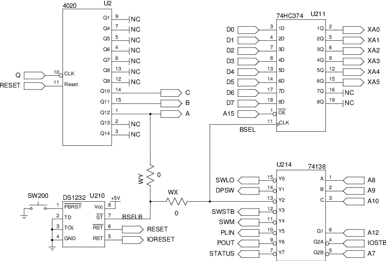
The second watchdog is located on the IO Board. The chip used is still a
DS1232 (U210) but the wiring is a little bit different. Firstly, since
there is no code running on that board, the reset pin of the U210 is not
connected to a CPU but to all registers (8-bit D flip-flop) which drive power
transistors.
Secondly, there is no reset pushbutton on the IO Board. The PBRESET pin is
connected to the BRESET signal coming directly from the CPU/Sound board.
So, if the first DS1231 triggers a reset signal, it automatically overrides
the second watchdog timer and forward the signal to all IO Board components.
However, this is not reciprocal: the IO Board cannot stops the CPU/Sound Board.
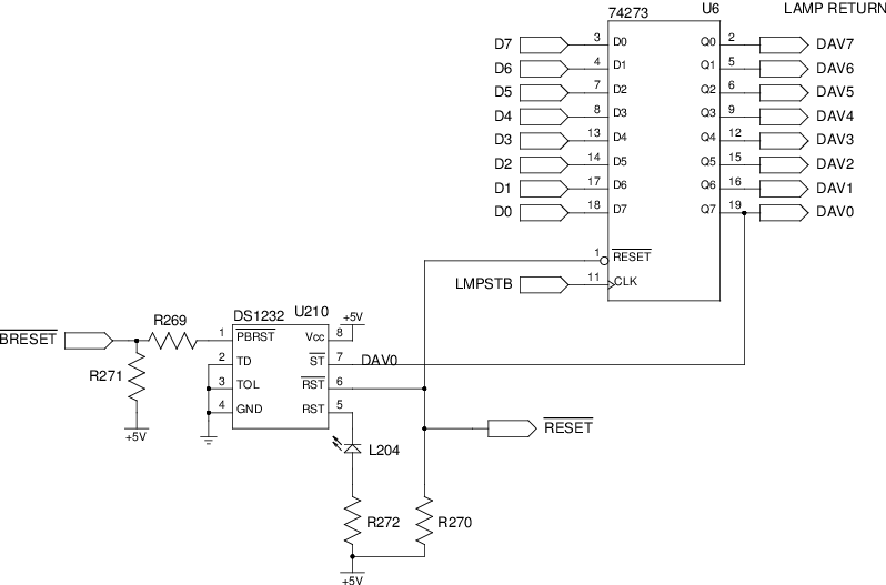
The strobe input of this watchdog is directly connected to the DAV0 signal
which is used to ground the first raw of the lamp matrix. This means that the
firmware has to frequently scan it to keep the IO Board alive. Tricky, but
not fully irrelevant since the lights are still blinking on this kind of
arcade machine in order to keep the game catchy.
All of this reset circuitry have to be kept in mind when developing a firmware for this kind of platform.
Final code
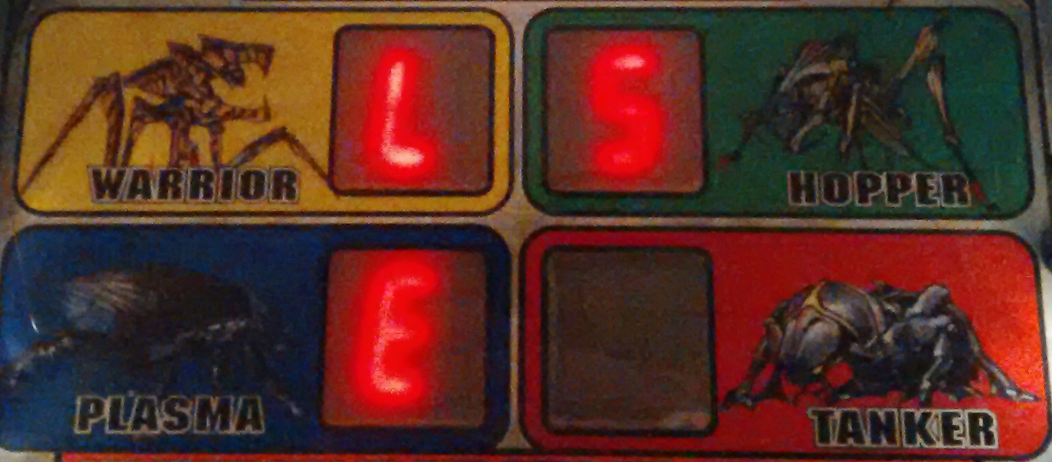
After many hours spent to reverse engineer the hardware part of this machine, I was finally able to print LSE on the 7-segment display of the playfield thanks to the code fetched from a custom flash ROM.
Here is the assembly code of my own basic firmware:
LAMP_ROW EQU $2008
LAMP_AUX EQU $2009
LAMP_COL EQU $200A
BANK_SELECT EQU $3200

;; CPU/Board Watchdog reset
wdr            .MACRO
                clra
                sta BANK_SELECT
                .ENDM

;; Dummy delay subroutine
delay           .MACRO i
                lda i
@l:             deca
                bne @l
                .ENDM

;; Entry point
                .ORG    0xC000
main:           ldx #lamps
                clrb
                stb LAMP_AUX    ;; Clear auxiliary rows
                incb            ;; Select first row

loop:           clra
                sta LAMP_ROW
                sta LAMP_COL    ;; Clear rows and colunms
                delay #$1F      ;; Dummy delay

                lda ,x+         ;; Fetch columns value
                sta LAMP_COL    ;; Set columns
                stb LAMP_ROW    ;; Ground selected row

                delay #$1F      ;; Dummy delay
                wdr             ;; Watchdog reset

                lslb            ;; Select next row

                bne loop        ;; Branch if the first 8 rows are not updated
                bcc main        ;; Branch if the 9th row is updated

                rolb
                stb LAMP_AUX    ;; Select the 9th row
                clrb
                bra loop

;; Lamp matrix values
lamps:
                DB $01, $00, $00, $00, $00
                DB $00, $1C, $B6, $9F, $00

;; Interrupt vector table
                .ORG    0xFFFE
reset:          DW main
tpasm is needed to assemble the preceding code and turn it into an Intel hex
file using the following commands:
$ tpasm -P 6809 -o intel cpu.hex cpu.s
$ hex2bin ./cpu.hex
$ dd if=/dev/zero of=cpu.rom bs=16K count=32
$ dd if=cpu.bin of=cpu.rom bs=16K seek=31
Conclusion
Hacking this kind of machine has been as rewarding for me as it is for some people to play flipper.
Unfortunatly, Sega Pinball left the market in 1999 (2 years after releasing
the Starship Troppers pinball…) and sold all pinball assets to
Stern Pinball, Inc. This company used the WhiteStar architecture until 2005
with NASCAR arcade machine. When The Lord of the Rings was released in 2003,
they edited some part of the sound system by replacing the
Motorola 6809 / BSMT2000 duo by a 32-bit Atmel AT91SAM ARM-based CPU and
three Xilinx FPGAs. So the 6809-BSMT2000 system is fully emulated by this
circuit to provide backward-compatibility.
Now that we have hacked the hardware, what about reverse engineering the original firmware? Maybe another time…
I hope you enjoyed this guided tour!