Designing an Intel 80386SX development board
The LSE-PC aims to be a compact IBM-PC compatible development board based on an
Intel 80386SX CPU and an Altera Cyclone IV EP4CE22E22 FPGA in order to
emulate a custom chipset.
The main goal of this project is to create a simple, debuggable and customisable version of the well-known PC hardware architecture. Its purpose is mainly didactic for students or experienced developers who want to get started into x86 low-level programming.
Hardware Overview
The schematics were designed using gschem which is a part of the gEDA project. Although the provided component library is acceptable, most of the chips used on this board are outlandish and so need to be drawn before starting overall schematics. This rude work was achieved by using djboxsym tool which allows quick production of gschem symbols from a minimal description.
Central Processing Unit
The CPU used on this board is a 80386SX designed by Intel and released in
- It is basically a cut-down version of the original
386with a 16-bit physical data bus. Although memory access performance is hardly affected, it is still fully 32-bit internally and was designed to be used in a 16-bit environment which is simpler and cheaper to design that a full 32-bit compatible motherboard. The physical address bus is only 24-bit which limits address space to 16MB.
The model used here is an NG80386SXLP20 which is a low power version
clocked at 20MHz and packaged in a 100-pin Plastic Quad Flat pack. Of course,
this chip is today considered obsolete but is still the only 32-bit x86 CPU
which is simple enough to be integrated in an amateur board.
Field-Programmable Gate Array
The main criterion for choosing an appropriate FPGA was about packaging.
Knowing that this chip will be hand-soldered, selecting a Ball Grid Array based
component was inconceivable. I’m also quite used to work with Altera’s FPGA so
one from the Cyclone IV series was a good compromise. The model chosen is an
EP4CE22E22C7N released in 2009. With its 22320 logic elements, it is one of
the largest FPGA available on EQFP. This package, only used by Altera, is an
enhanced version of the standard plastic quad flat package which uses a step of
0.5 millimeter between each pins. This layout allows the FPGA to expose 144 pins
where 62 can be used as I/O and 15 as clock inputs.
An other useful feature is the 3.3V PCI compliant mode of the IO banks. It provides compatibility with 5V devices by enabling a clamping diode which can supports 25mA. This explains the use of 120 Ohms resistors between CPU 5V signals and FPGA IO.

The CPU needs a 20MHz input clock to operate correctly. A unique oscillator is used to clock CPU and FPGA. The idea here is to assume that if the FPGA needs a higher clock speed, the use of an internal Phase Locked Loop will be considered to obtain the desired frequency from this 20MHz clock.

FPGA programming and debugging can be performed through JTAG. Altera provides a dedicated programmer called the USB Blaster which can be easily used with Quartus II. It provides a standard 10-pin connector and operates here at 2.5V.
As FPGA configuration is volatile, it is necessary to provide an external way
to program it when the board is powered on. Here this is achieved by an external
serial flash which contains the whole FPGA configuration. Altera sells EPCQ
devices which are dedicated to that purpose. However, most of the time those
are expensive and it turns out that they are nothing more than SPI flash
memories.
That is why it has been decided to use an M25P16, a 16Mbits flash memory from
Micron which perfectly do the job.
In fact, several programming modes are available in this FPGA. In order to
indicate what mode has to be used, MSEL pins must be pulled-up or pulled-down
to encode the mode number. To select the Active Serial Programming mode, it is
necessary to solder 120 Ohms resistors on R77, R79 and R81.

USB/UART bridge
In addition to JTAG, it can be a good idea to provide USB connectivity to this
design. However, implementing USB protocol stack in an FPGA can be really
painful. The purpose of the FT230X chip is to provide a simple bridge between
an USB and an UART interface which is simpler to implement in an FPGA. It is
provided in a SSOP16 package and is really simple to wire thanks notably to the
fully integrated clock generation which does no require an external crystal.

Static Random Access Memory
For the main RAM, AS6C8016 from Alliance Memory has been chosen. This is a
512K x 16-bit CMOS static RAM packaged in a 44-pin TSOP. It features tri-state
output and data byte control (LB and UB signals) as required by the
80386SX.
Although this chip was originally designed to be used as a battery backed-up
non-volatile memory, its usage simplicity and its response time justify the low
storage space. So 1MB ought to be enough for anybody. Also, AS6C8016 is
powered by 5V but is still fully TTL compatible which means that it can be
driven by the CPU as well as the 3.3V outputted by FPGA’s IO. So control signals
as RAMCS and RAMWE are only driven by the FPGA which will perform address
decoding.

Voltage Regulation
The power circuitry has to provide four sources of different voltages:
- 5V: CPU, SRAM
- 3.3V: FPGA In/Out
- 2.5V: FPGA Analog PLL
- 1.2V: FPGA internal logic, Digital PLL
Regulation is achieved by three fixed low drop positive voltage regulators which operate from the 5V supplied by the USB. Even though fixed regulators are often more expensive that adjustable regulators, they are easier to wire and reduce the number of passive components needed to perform adjustment. Only 250mA are provided for 2.5V because it is only used by FPGA Analog PLL and JTAG target voltage.

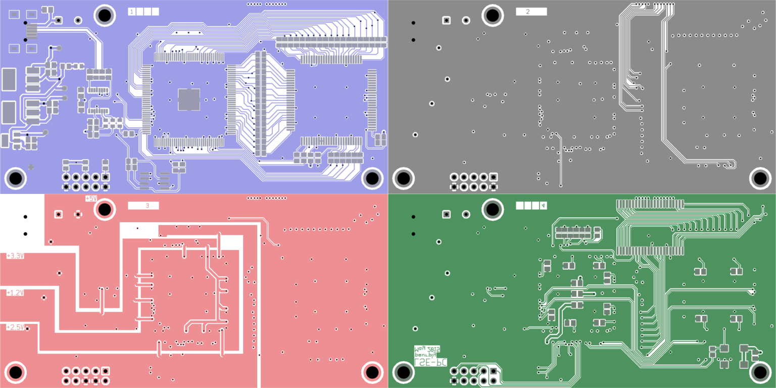
Routing and Manufacturing the Printed Circuit Board
Once the schematics completed, PCB has to be designed. This process has been assisted by pcb, an other part of gEDA project. As schematics and PCB designs are not performed using the same software (as KiCad or Eagle do), synchronization between those is ensured thanks to the gsch2pcb tool.
As some components on the board do not use standard packages, creating custom pcb footprint for those chip is necessary. Like symbols generation, footprints was generated using footgen.
The PCB routing here is a bit tricky due to the large number of signals needed to drive the CPU. A 4-layer PCB is unavoidable in order to achieve routing and to preserve signal integrity. As our manufacturer limits 4-layer board 5 x 10cm, this is the dimension adopted which is large enough for this design.
Each layer has a dedicated purpose:
- Top layer : it is mainly used for signals routing. Traces used for data signal are 0.20mm width which is the limit imposed by manufacturer. Unused spaces are recycled to ground planes. FPGA, CPU and voltage regulators are soldered on this layer.
- Ground layer : Used almost exclusively to get a common ground plane in the whole circuit. It has also been used to complete RAM routing.
- Power layer : Dedicated to conduct power rails through the board. Four areas corresponding to each voltage level can be clearly seen on this layer.
- Bottom layer : Like the top layer, this is mainly used for signals routing. Capacitors used to apply local filtering are soldered on this side as well as SRAM and 20MHz oscillator.
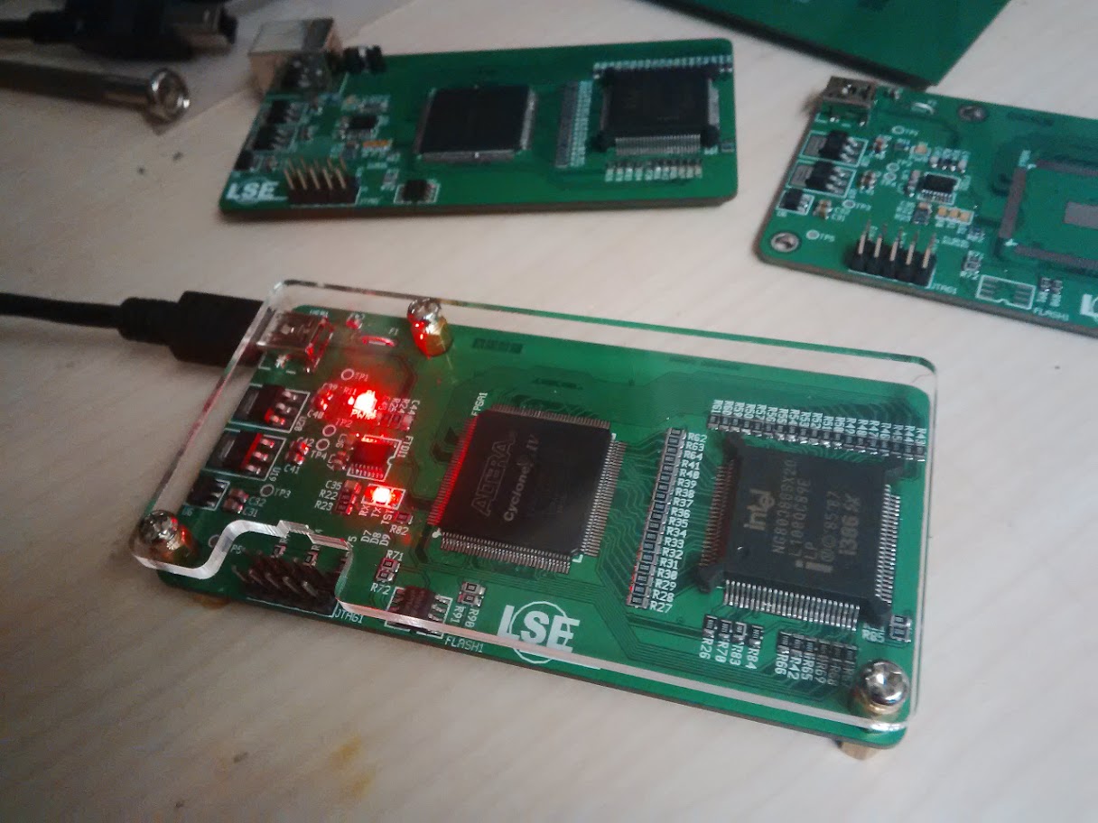
With a low end SMD soldering station, it takes approximately three hours to solder a whole board.
In addition to PCB, acrylic case was designed using FreeCAD and then manufactured.
Emulating a rudimentary chipset
Now that the board is correctly soldered, the last thing to do before being able to run code on the CPU is to configure the FPGA in order to emulate a basic chipset. The design is composed of two parts : the bus controller and the memory controller.
Bus Controller
The bus controller has to handle 80386SX bus access protocol. In order to
understand the exact purpose of it, it is necessary to detail signals involved
in the process.
- The Data Bus (
D[15:0]) is composed of three-state bidirectional signals providing a general purpose data path between386and other devices (such as memory). - The Address Bus (
A[23:1],BHE#,BLE#) is composed of three-state outputs providing physical memory addresses or I/O port addresses. The Byte Enable outputs (BHE#andBLE#) indicate which bytes of the 16-bit data bus are involved with the current transfer. If both of them are asserted, then 16 bits word is being transferred, - A Bus Cycle is defined by
W/R#,D/C#,M/IO#andLOCK#three-state outputs.W/R#distinguishes between write and read cycles,D/C#distinguishes between data and control cycles,M/IO#distinguishes between memory and I/O cycles and#LOCKindicates if the current operation is atomic or not. - The Bus Access is controlled by
ADS#,READY#andNA#. The Address Status (ADS#) indicates that a valid bus cycle definition and address are being driven from the386pins. Most of the bus controller logic must be based on the falling-edge of this signal.READY#signal indicates a transfer acknowledge driven by the bus controller to the386.NA#signal is used to request address pipelining which is not relevant in this case.
As an example, here is a waveform of bus signals during these operations :
- Write data1 to address1
- Read data2 from address2
- Write data3 to address3
- Idle
- Read data4 from address4

Each bus access operates in two steps. The first one, indicated by ADS# is
used to drive Bus Cycle Definition signals and an address. The second one take
place during the next rising edge of the main clock. Depending on the W/R# pin
state, the data bus is driven with the value the CPU wants to write. During all
these sequences ADS# is still asserted.
The next bus cycle is performed when the 386 detects a falling edge on the
READY# signal. So the bus controller can be easily modeled as the following
Finite-State Machine :

It is simple to implement this behavior in Verilog :
always @(posedge clk)
begin
    if (!_ads) begin
        capture_bus(); // Capture values driven on
                       // A[23:1], D[15:0], /BLE, /BHE, WR, DC and MIO
        _ready <= 1;
        state <= `ST_T1;
    end else if (state == `ST_T1) begin
        _ready <= 0;
        state <= `ST_T2;
    end
end
As data bus is bidirectional, it is sometimes necessary to set it in high
impedance in order to let another device driving the bus. It is also needed to
respect bytes requested by the CPU via BHE# and BLE#.
assign d[15:8] = wr || _bhe || !ramcs ? 8'hzz : dout[15:8];
assign d[7:0] = wr || _ble || !ramcs ? 8'hzz : dout[7:0];
Memory Controller
Once the bus protocol is properly respected, the address requested by the CPU must be decoded in order to figure out which device must be selected. This is here the purpose of the memory controller unit.
Altera Cyclone IV devices features embedded memory structures. It consists of M9K memory blocks that can be configured to provide various memory functions, such as RAM, shift registers or ROM. The idea here is to use it to create a small memory which is initialized with a basic piece of code dedicated to CPU initialization. An other useful feature of this memory is to be easily readable and editable through JTAG using the In-System Content Editor provided by Quartus II.
Basically, the main address space is composed of two memories : an external (i.e. the SRAM) and an internal (i.e. the M9K blocks).
The first megabyte of addressable memory is organized as the layout of the
traditional IBM-PC. It means that only the first 640K of external memory are
mapped from 0x000000 to 0x0A0000 and BIOS shadow ROM (implemented here
with internal memory) is mapped from 0x0F8000 to 0x100000. Shadow ROM was
originally a 64KB memory which contains a copy of the BIOS ROM mapped on the
last 64KB of the address space. As the CPU starts fetching instructions at
0xFFFFF0 after a reset, the mechanism consists of mapping a ROM at this
address, copying ROM content on the shadow ROM and then jumping on a subroutine
located on the first megabyte.
Here, the internal RAM is only 32KB due to the FPGA limitations and is located
at 0xFF8000 and 0x0F8000 which allows simulation of the original machinery.
Moreover, the whole SRAM is mapped from 1MB which means that first 640KB of
external RAM are mapped twice.
Memory controller unit can be simplified as :

The actual address space layout is achieved by applying a logic expression
to the chip select signal of each memory. Notice that WE# signal of SRAM
is not active on the same level that W/R# 386 signal. So this signal is
inverted by the FPGA.
assign eramwe = !wr;
assign eramcs = !(cs && ((addr[23:16] < 8'h0A)
                 || (addr[23:20] == 4'h1)));
assign iramcs = cs && ((addr[23:15] == 9'h1FF)
                || (addr[23:15] == 9'h01F));
Skeleton of a basic firmware
As an example, this section will present a basic firmware which can be run on the LSE-PC.
Firstly, it is considered here that the entire firmware will be located on the internal memory which is automatically initialized when the design is loaded into the FPGA.
On reset, the 80386 CPU is running in real mode and will start to execute
the instructions located at the end of the address space: 0xFFFFF0. So the
purpose of these instructions are to jump to the first megabyte by reloading
Code Segment. However, the last 16 bytes can be used to set a minimal
environment to allow 16-bit application execution. The following code is an
example of 5 instructions that can be assembled to 16 bytes of opcodes. It
basically sets Data, Stack and Code Segment Selector, sets the stack
pointer and then jumps to the beginning of the internal ram mapped at
0x8000.
org 0xFFF0  ;; CS:0xF000, IP:0xFFF0
reset:
        mov ax, 0xF000
        mov ds, ax
        mov ss, ax
        mov sp, 0xFFF0
        jmp 0xF000:0x8000
Now that the execution flow has exited the reset state, it is now possible to
set the CPU to protected mode. This can be achieved by loading a simple Global
Descriptor Table which defines memory segments that will be used in protected
mode. Notice that the jump to reload_segs is used to flush instruction
the prefetch queue after enabling protected mode in order to validate segment
reloading. This code can be improved by the setting of an
Interrupt Descriptor Table in addition of a Global Descriptor Table.
org 0x8000
startup:
        lgdt [gdtr]             ;; Load Glocal Descriptor Table

        mov eax, cr0            ;; Enable protected mode
        or eax, 1
        mov cr0, eax

        jmp reload_segs         ;; Flush prefetch queue

reload_segs:
        mov ax, 0x10            ;; Reload segment selectors
        mov ds, ax
        mov es, ax
        mov fs, ax
        mov gs, ax
        mov ss, ax

        ;; ljmp 0x08:0xF8400
        dw 0xEA66               ;; Reload CS and jump to application code
        dd 0xF8400
        dw 0x08

align 16
gdt:    ...
gdtr:
        Limit dw gdtr - gdt - 1
        Base dd 0xF0000 + gdt
A 32-bit application can then be located at 0xF8400. The internal RAM is segmented according to the following layout :

As the In-Sytem Memory Content Editor accepts a special binary format called MIF (Memory Initialization File), a dedicated OCaml script has been created to facilitate linking of several raw binary object files.
bin2mif -o fw.mif
    -b 0xF8000 0 \              # Memory base address
    -i pm.bin 0xF8000 0 \       # Jump to protected mode code
    -i app.bin 0xFC000 0 \      # Application code
    -i reset.bin 0xFFFF0 0      # Reset routine code
Providing debug facilities
Even though Altera’s FPGA provide an efficient internal signal analyser thanks
to SignalTap, it is a real pain to make software debugging when the size
of applications running on the 386 become significant. Adding a flexible
on-chip debug facility based on the UART communication to this design is one of
the main challenge of this project.

Supervisor
The supervisor is designed using Altera’s QSys tool which assists the creation
of systems based on the NIOS II soft-processor. This system is composed of a
private on-chip memory which contains NIOS instructions and data, and of an
UART which is connected to FT230X chip.
The protocol between the host and the supervisor is pretty simple and it considers that the CPU is at any time in one of these states :
STOP: CPU is stopped.RESETsignal is asserted.RUN: CPU is running.IORD/IOWR: CPU is trying to perform an access to IO ports. Distinction between read and write operation is done. Those states are used to allow device emulation.BRK16/BRK32: CPU is ready to accept debug operations. Distinction between real and protected mode is done.
It is accurate to implement the protocol logic through NIOS software instead
of having it hardwired in Verilog. However, directly handling 386 signals on
the NIOS is inefficient due to execution speed of this system. The idea here
is to export the 386 signal handling job to an other module dedicated to it :
the On-Chip Debug Unit.
The OCD Unit can take the control of 386 buses at anytime by asserting the
ocd.en signal, which disable the original bus controller described before.
The communication between those two units is ensured by a dual-port shared
memory accessible through Avalon bus and two PIO registers. The first one,
OCD_CTL, is used to reset the OCD Unit from supervisor. The second,
OCD_STATUS indicates if the unit is running or not. The shared memory
contains a routine that must be applied on 386.

On-Chip Debug Unit
This unit is basically a processor specially designed to handle 386 signals.
It fetches its instructions from the 256 x 16-bit Avalon memory filled by the
supervisor and operates on a 16 x 16-bit data space also located on shared
memory.
While supervisor can access OCD program and data unrestrictedly, the
OCD Unit can only operates on its data space which corresponds to offset
0x100 from supervisor point of view. In the dedicated assembler, data memory
is addressed using R1 to R15 naming convention.
module ocd
(
    // OCD Control
    input rst,          // Connected to OCD_CTL
    input clk,          // 40MHz clock (synchronous with 20MHz CPU clock)
    output reg en,      // Asserted if OCD Unit is attached to the 386
    output reg stop,    // Connected to OCD_STATUS

    // 80386 signals
    ...
    // RAM signals (Avalon)
    ...
);
Implementing this kind of processor is quite simple and a basic one will be based on the following state machine :

As Avalon memory signals are always latched, reading on it takes two clock cycles : the first cycle is used to latch the address value and the second one latches the result on the data bus. Taking that into account, execution of a single instruction which reads and writes on data memory cannot take less than five clock cycles.
- FETCH : Get instruction from program memory.
- LOAD : Latch source address into data memory.
- EXEC : Load source value from data memory and execute the instruction.
- STORE : Store result and compute next address of the next instruction.
- LATCH : Latch instruction address into program memory.
Instruction set is composed of several categories. The first one is used to control the OCD :
ATTACH/DETACH: Connect/Disconnect the OCD unit to 386 signals.
The second category includes instructions related to 386 signals processing :
LDD d: Load data bus value intodregister.LDAL d/LDAH d: Load address bus value intodregister.LDWR d: LoadW/R#signal intodregister.LDDC d: LoadD/C#signal intodregister.LDMIO d: LoadM/IO#signal intodregister.STD s: Set data bus value tosregister value.START/RESET: Start/Reset the CPU.READY: AssertREADY#signal.
Of course, some instructions only operate on registers :
LDI d, imm16: Load a 16-bit immediate intodregister.MOV d, s: Movesregister value intodregister.CLR d: Cleardregister.
Third category is about flow control. As the data memory only exposes one port to the OCD Unit, implementing a compare instruction which loads two registers is not possible in a single cycle. So a compare register as been added to the core. All comparisons will be related to that register.
LDCMP s: Loadsregister value into the compare register.CMP s: Comparesregister value with compare register value and store the result into the compare register.BA/BEQ/BNE addr: Branch to the specified address according to compare register value.
As example, those instructions performs a jump to label if R1 is equal to R2 :
    LDCMP R1    ;; cmpr <- R1
    CMP R2      ;; cmpr <- cmpr == R2
    BEQ label   ;; pc <- label if cmpr != 0
Some instructions can stay more than one cycle in the EXEC state order to wait for an acknowledge from the CPU during some bus operation :
HOLD: AssertHOLDsignal and wait forHOLDAsignal.INT: AssertINTsignal and wait forINTAsignal.EXIT: Stop OCD routine execution. Never leaves EXEC state and assertocd.stopsignal.
This wait state mechanism is also used to implement instructions used to wait
for a particular event on the bus. All those instructions deassert READY#
signal and attach the OCD to the 386 when the expected condition is
triggered.
WAITADS: Wait forADS#signal to be assertedWAITIO: Wait forADS#andM/IO#getting lowWAITLOCK: Wait forADS#andLOCK#to be asserted
The block diagram of this unit can be represented as :

Here is routines used to reset and start the CPU from OCD Unit. Notice that
the start routine let the original bus controller operates on the 386 until
an IO access is performed. The supervisor has just to be interrupted when the
OCD is exited from the start routine to handle the IO request. Devices can
then be emulated by the supervisor or by the host.
.func ocd_prgm_reset
    RESET           ;; RESET <- 1
    EXIT

.func ocd_prgm_start
    START           ;; RESET <- 0
    DETACH          ;; Let bus controller to handle CPU signals
    WAITIO          ;; Wait for IO access to attach OCD Unit
    LDAL R1         ;; Get IO port address
    LDWR R2         ;; Get IO operation type
    EXIT
Example : Obtaining CPU registers
Now that the OCD Unit internals have been presented, the purpose now is to use it to get CPU registers.
Before applying debug operations on the CPU, it is necessary to stop execution
and set it up in a known state. The simplest method to interrupt a 386
without having to mind about the interrupt flag is to send a Non
Maskable Interrupt. Unlike INTR signal, NMI mechanism does not provide any
acknowledge from the CPU. So the way only to know if the CPU actually took into
account the NMI is to wait LOCK# signal assertion. Indeed, the 386 locks
the whole bus when it accesses an IDT or IVT entry. The WAITLOCK
instruction has been designed for that specific purpose.
    .func ocd_prgm_break
    NMI             ;; Set NMI signal
    WAITLOCK        ;; Wait for ADS# and LOCK# signals then attach OCD unit

On the next step, the behaviour of the CPU is different according to its mode.
If the 386 is still in real mode, it will fetch the code segment and the
offset of the NMI handler located on the Interrupt Vector Table. As IVT
always starts at 0x0000000, the address 0x0000008 will be outputted after
triggering the NMI.
In the other hand, if protected mode is enabled, the CPU will fetch an Interrupt Descriptor corresponding of the NMI interrupt. This structure is located on the Interrupt Descriptor Table which can be found anywhere on the address space.
As the processor mode is unknown at that moment, it can be deduced from the first requested address after NMI :
;; Get CPU Mode
    LDAL R2                     ;; Load requested address
    LDAH R3
    LDCMP R2
    LDI R1, 0x0008
    CMP R1
    BNE break_protected_mode    ;; Branch to protected mode handler if
                                ;; A[15:0] != 0x0008
    LDCMP R3
    BEQ break_real_mode         ;; Branch to real mode handler if
                                ;; A[23:16] is equal to the NMI entry
                                ;; offset on the IVT
Only protected mode will be considered for the rest of the example.
As IDT set by the application cannot be trusted, using the OCD Unit to drive a valid interrupt gate is conceivable :
;; Fake IDT entry
    LDI R1, 0b1000111000000000      ;; Flags
    STD R1
    WAITADS
    LDI R1, 0x000D                  ;; Offset[31:16]
    STD R1
    WAITADS
    LDI R1, 0x0000                  ;; Offset[15:0]
    STD R1
    WAITADS
    LDI R1, 0x0008                  ;; Segment Selector
    STD R1
    WAITADS
A code segment reload is always performed before jumping to the interrupt handler. So a read to a GDT entry will be requested by the CPU.
In the same way, it is painless with this mechanism to drive a valid code segment :
;; Fake GDT entry
    LDI R1, 0b1001101000000000  ;; Flags | Base[23:16]
    STD R1
    WAITADS
    LDI R1, 0x00CF              ;; Base[31:24] | G | D/B | Limit[19:16]
    STD R1
    WAITADS
    LDI R1, 0xFFFF              ;; Limit[15:00]
    STD R1
    WAITADS
    LDI R1, 0x0000              ;; Base[15:0]
    STD R1
    WAITADS
    READY                       ;; GDT Access bit
    WAITADS
Finally, as EFLAGS, EIP and CS registers have been modified, they are
pushed on the stack. However the bus controller is disconnected from CPU
signals : this means that no actual write on the memory are performed during
this operation. Instead, it is straightforward to load those values into OCD
registers :
;; Context saving
    LDD R2          ;; EFLAGS[15:0]
    READY
    WAITADS
    LDD R3          ;; EFLAGS[31:16]
    READY
    WAITADS
    LDD R4          ;; CS
    READY
    WAITADS
    LDD R5          ;; EIP[15:0]
    READY
    WAITADS
    LDD R6          ;; EIP[31:16]
    READY
Afterwards, the CPU will try to fetch instructions from the interrupt handler.
So HOLD signal is asserted at the end of the break routine. This leaves the
supervisor time to load the next routine to the OCD program memory.
At this point, 386 is on a known and valid state which allows us to inject
any instructions sequences. In order to obtain CPU registers, the pusha
instruction can be injected :
    .func ocd_prgm_get_regs
    LDI R1, 0x9060
    LDI R2, 0x9090
    WAITADS

    ;; Fill instruction prefetch queue
    STD R1          ;; Drive PUSHA; NOP
    WAITADS
    STD R2          ;; Drive NOP; NOP
    WAITADS
    STD R2          ;; Drive NOP; NOP
    WAITADS
    STD R2          ;; Drive NOP; NOP
    WAITADS
    STD R2          ;; Drive NOP; NOP
    WAITADS

    ;; PUSHA
    LDD R0
    READY
    WAITADS
    ...
    LDD R15
    READY

    HOLD            ;; Hold CPU in order to avoid instruction fetch during
                    ;; loading of the next OCD routine
    EXIT
However, pusha instruction modifies ESP value. In the same way, a mov
instruction can be used to restore ESP and set any register value.
When debugging phase is over, a continue routine is executed which basically
inject an iret and drive original values of EIP, CS and EFLAGS.
For now, the debug unit is provided with a CLI interface allowing simple CPU interactions. When more debug features will be available, the goal is to embed a gdb stub into the host application.
[lsepc-monitor] start
[lsepc-monitor] status
CPU Status: RUN
[lsepc-monitor] break
[lsepc-monitor] status
CPU Status: Break (Protected Mode)
[lsepc-monitor] getregs
EFLAGS: 00000046
EIP:    000fd024
ESP:    ffe4000c
EBP:    00000123
EAX:    1100bbaa
EBX:    5544000f
ECX:    9988ffee
EDX:    ddcc7766
ESI:    456789ab
EDI:    cdef9090
CS:     0008
[lsepc-monitor] continue
[lsepc-monitor] status
CPU Status: RUN
Conclusion
Developing and testing on the LSE-PC is still mainly based on the JTAG interface. When connected to a JTAG interface, the FPGA design exposes the following entry points :
- RAM/ROM editor : used to perform on-chip operation on the internal memory
- NIOS II interface : used to program and debug the NIOS II contained on the supervisor
- Serial Flash Loader : used to program the SPI flash which contains FPGA configuration
- SignalTap : used to perform signal analysis.
This board is still a proof a concept. However, its composition was an
excellent exercise to understand how the original 80386 CPU works under the
hood.
Although some work need to be done to get a profitable on-chip debugger, the hardware part and the simple chipset embedded are reliable enough to allow execution of simple applications.