One Device to drive them all
Prologue
Three Devices for logic analysis of passively captured traces,
Seven for inter-chip communication driven by hardwired interfaces,
Nine for in-circuit debugging limited to specific purpose,
One for complex hardware hacking scenarios.
Three tinkerers took those words as they are. Overthrown by the complexity implied by the multiplicity of inefficient tools, they thought that time had come to undertake this problem from another angle.
All they needed was a simple way to manipulate the exotic devices that they required for their projects. Manufactured by foreign organizations, devices referred here were designed to fulfill a predefined purpose and were intended to be used as black boxes. Without any knowledge of the internal mechanisms involved in their operations, it was conceivable to integrate them if they were in the kind of environment that they were promised to.
But those tinkerers though differently. Their situation was mostly complicated by the fact that they had already acquired a good control of their personal computers that they considered as their main and perfect workstation. Well defined and roughly understood, they were too stubborn to learn another way to work as they unanimously decided that this method was the most effective and compliant with the rest of their work.
So instead of reworking there methodology, they agreed that defining a third device whose only purpose was to handle the interfacing between the workstation and the device under test were inescapable. The first member of the group asked to others what options were available to fit this position.
The second one said that he already made an intensive usage of the Arduino for that. Providing an easy access and control of its GPIO and some hardwired bus controllers, it was suitable for the most simple cases.
The third one discussed the merits of the Bus Pirate from Dangerous Prototype. Mature and widely-used, this tool provided a direct control of its interface via USB without the need to develop a specific firmware to be actually used.
The first one replied to these proposals that they had a common issue: they simply performed the communication with the host by using an interface based on the translation of USB to UART speeded at 115200 bauds. For him, it prohibited a fine-grained configuration and then limited the full capacities provided by the USB protocol.
They all agreed on this last point and started to work on a first prototype of their response to this situation.
It was based on a STM32F072 microcontroller and mapped SPI, I2C, UART and CAN signals to physical headers. As this chip was able to drive USB signals, a USB mini-connector was directly connected to it.
Concerning the software side, one interesting idea here was to expose the hardware interfaces using the corresponding subsystem in the Linux kernel. Even though these subsystems were mostly used to describe on-chip interfaces, adapting them to wrap up the USB functions was feasible. For instance, the SPI exposed by the device could be manipulated as a regular spidev.
Although the concept of such board was appealing at the time, limitations quickly appeared. First of all, most of the USB protocol had to be implemented via software on the STM32F072 which led to a significant overhead on each USB transaction. Secondly, fully implementing the host driver in kernel space implied a rigid configuration and error-prone if not implemented correctly. Finally, the global stability of the STM32F072 MCU was quite poor especially during a development phase where on-chip debugging had to be frequently used.
One year passed and no one was actually enthusiastic to use this dead-born project in a real context. The first one, whose credibility was at its lower point, got the bravery to propose to the two others to rethink the project from the beginning. And they accepted, against all odds.
This write-up must be considered as the collection of thoughts that led them to the design and the manufacture of a second version of this small, unpretentious, and unfinished electronic board.
Chapter I: Forging the One Device
The first step for them was to clearly define how and what could make the second version of the board better than the previous one. The main issue was related to the lack of flexibility of the design and they wondered how they could handle a protocol not supported by the microcontroller they used.
Then they decided to take a look at the wide range of Programmable Logic Devices available nowadays. As a first prototype, a CPLD appeared to be the best choice for such application. Compared to a regular FPGA, these non-volatile PLD were cheaper and required a much more simpler configuration circuit. They also thought that the prototype was designed to only prove a concept and moving to a more powerful FPGA for next versions was conceivable.
Section I: From Ink…
From a high-level point of view, the board had been specified to expose a reasonable number of IOs directly connected to a controller, here an Altera Max V CPLD. As the flaky soft USB implementation of the previous version was quite inconvenient to maintain and to keep reliable, the job here had been assigned to a well-known and solid dedicated USB controller: the FX2LP from Cypress Semiconductor. This highly integrated USB 2.0 microcontroller implemented most of the protocol logic in silicon and only burdened its integrated 8051’s firmware with the high-level configuration aspect of USB.

And then came the question about the communication between the USB controller and the IO controller. The FX2LP embedded a powerful mechanism to forward the content of a USB entrypoint to an hardware FIFO without any interaction with the internal 8051. These EP buffer’s words could then be dequeued by an external component using an hardware interface.
However, this one was defined by a 16-bit data bus and 6 control signals which was quite pin-consuming for the CPLD they chose. Fortunately, another mechanisms offered by the FX2LP allowed the programming of a custom protocol to transmit and receive these data with the external world: the General Programmable Interface. As for the regular FIFO interface, this hardware unit was almost completely independent from the 8051. The firmware was only responsible to program the hardware state-machines used to represent the waveforms of a one-word transmission.
In their case, they chose to allocate 8 wires for the bidirectional data bus, 3 control signals driven by the USB controller and 2 ‘ready’ signals initiated by the IO controller. At that point, none of them had actually thought about the exact shape of the waveforms and the purpose of the control signals but planned to consider that once the first board would be fully manufactured.
The USB device interface was composed of 3 endpoints. The endpoint 0 acted as a regular control endpoint and was used to transfer small requests. Meanwhile, endpoints 2 and 6 were dedicated to bulk transmissions and receptions respectively. The two last were directly connected to the internal FIFO while the first one was completely handled by the 8051.

To power these components, the 5V supplied by the USB were firstly shifted to 3.3V using a low-dropout voltage regulator to power the USB controller and the IO banks of the CPLD while a 1.8V regulator powered the CPLD’s internal logic.
The main clock was managed by the FX2LP. Connected to a 24MHz crystal, the internal PLL were configured by the 8051 firmware allowing a CPU clock frequency of 48MHz, 24MHz or 12MHz. As the output of the phase-locked loop was also exposed outside the USB controller by the CLKOUT pin, the CPLD used it as a system clock.
The GPIF unit had a dedicated clock that could be fed internally or imposed by an external device. All operations on this interface were aligned to this signal. In order to avoid to deal with multiple clock domains in the CPLD, they arranged to drive the IFCLK signal from the IO controller at the half frequency of the system clock.
An I2C EEPROM had been connected to USB controller in order to store its firmware in a persistent way. The internal reset logic of the FX2LP was designed to scan the I2C bus for EEPROM from where a valid firmware could be loaded. Once the program was fully copied to internal RAM, no operations were performed on this bus.
After several tries, they finally validated the following schematic:

Section II: …To Copper
Once the design approved, the next step consisted to draw the printed circuit board. Two layers were enough to route the entire netlist in a surface of 5x5cm.
The top layer was dedicated to voltage regulation, CPLD, connectors and a couple of switches and LEDs. Meanwhile, the bottom one contained the whole circuit required to make the USB controller working: crystal, EEPROM, I2C pull-up resistors, …
IOs from the CPLD were exposed via 2 dual-row 20-pin female headers of 2.54mm pitch.
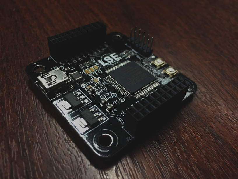
As the board was manually soldered, it was not conceivable for them to use BGA components for this prototype. So the 100-pin LQFP version of the CPLD had been used as well as the 56-pin SSOP package of the Cypress’s chip.
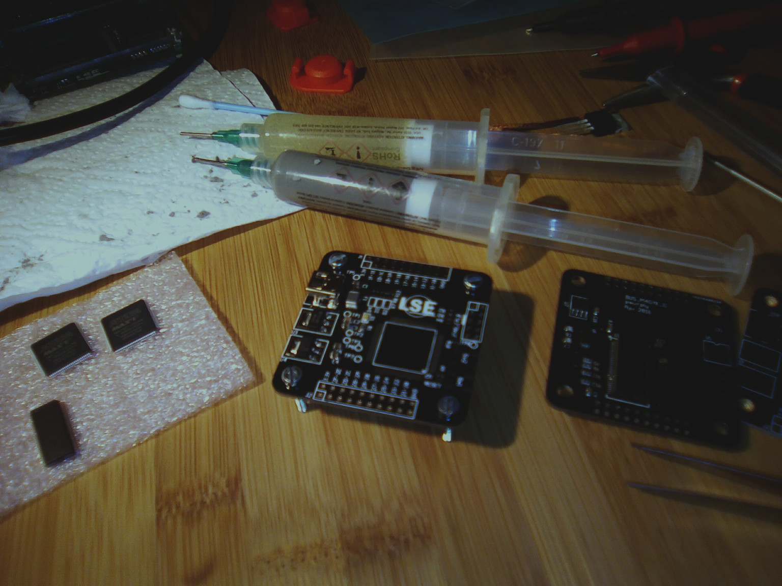
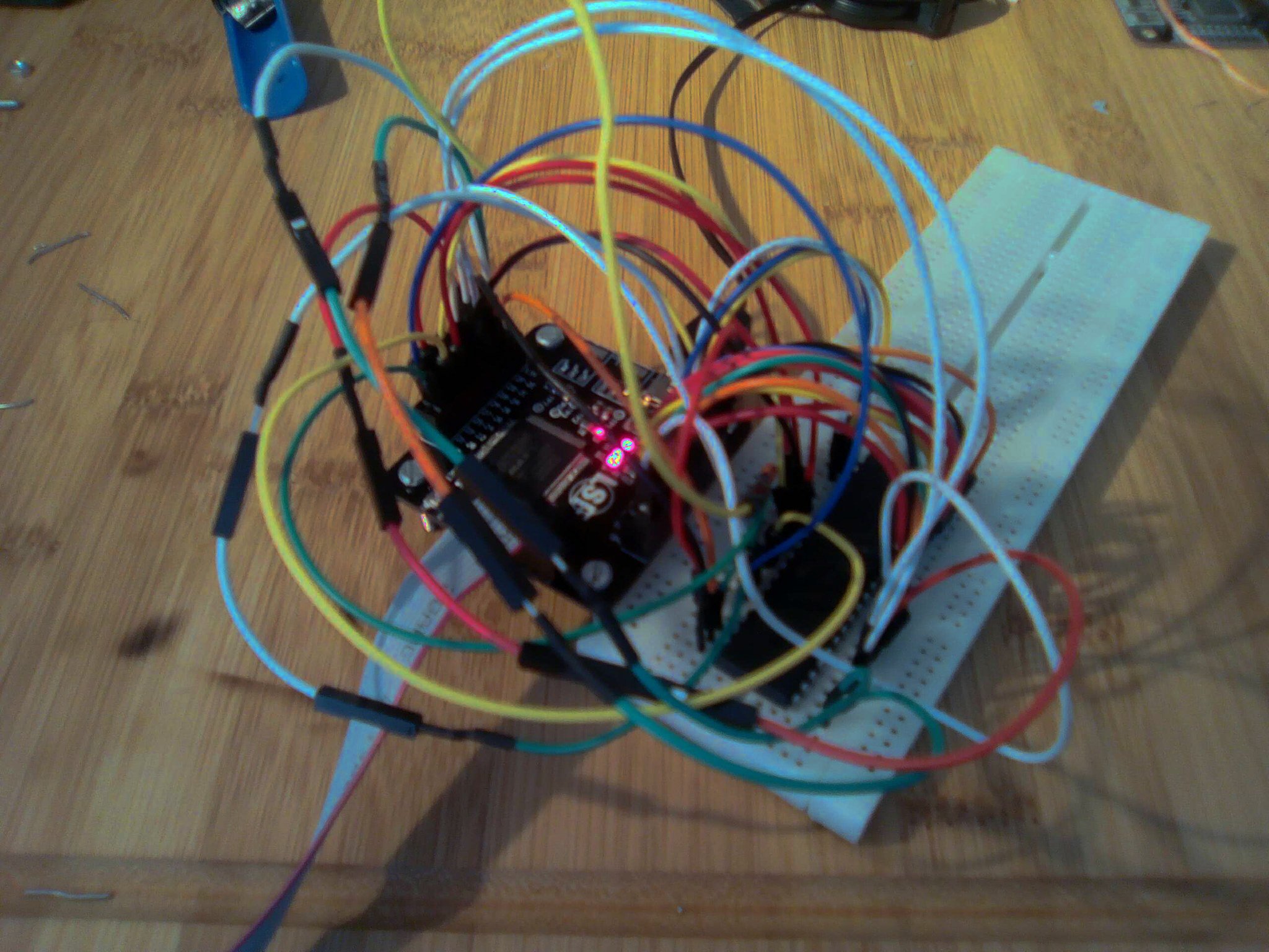
After hours of painful electrical tests, a first sample of a fully soldered board was born by the end of the Spring:
Chapter II: On Reprogrammability They Hoped
Although the physical board was ready, a firmware was still needed to make it working. The situation was more complex than just a simple binary located in a single ROM as most of the boards of this category are.
First of all, the firmware for the FX2LP had been implemented which basically consisted to configure the USB and the GPIF units of the chip. Nothing uncommon here: writing applications for this kind of microcontroller was quite easy as it was well-documented and that tons of similar usages of this chip already existed and were publicly available. The code has been written in a couple of hours and no new features have been added since as they decided to make the firmware serving only one unique purpose: translate USB data to IO controller in the most simple and lightweight way.
For them, most of the customizations that would be needed should be fully-implemented at the IO controller level. The real challenge here was to take advantage of the CPLD as a powerful and programmable IO controller.
One solution would be to base the CPLD’s design on a soft-processor: modifying IO’s behaviour would mean loading a new firmware into its RAM. Although this architecture was quite common when using an FPGA, it became more inconvenient when basing it on a CPLD due to the lack of memory blocks.
The second solution would be to generate and configure the design of the CPLD according to the user’s needs dynamically. As pursuing this concept using a regular hardware description language seemed almost impossible for them, they decided to fully base the design generation on Migen. This python module allowed the meta-programming of synchronous register transfer level design and handled the generation of a verilog file that could then be synthesised by the regular Altera’s toolchain.
Section I: Modularity And Modulation
They fully defined the architecture around the concept of modularity. To demonstrate how it would transpire in a real context, they took the example of a Pulse-Width Modulation interface.
The main principal of such technique was to use a rectangular pulse wave whose pulse width was modulated resulting in the variation of the average value of the waveform.
A possible implementation of a PWM module could be achieved by using a counter whose width defined the period of the signal and a digital comparator to generate the needed duty cycle.
In this case, the only signal that was likely exposed externally would be the output of the comparator, negated or not. Moreover, a ‘parameter’ of this circuit would be the left-input of the comparator and was typically the kind of signal that would be interesting to implement as a register writable from the host.
For their example, they also considered that the counter value could be watched from the host.

The ‘parameter’ signals were called ‘Control Registers’ and were intended to be readable and/or writable from the host while the signals that would be eligible to be mapped to a physical pin of the CPLD were called ‘IO Signals’.
In a more generic way, this kind of module, that they called ‘IO Module’, could always be represented according to the following template:
-
An internal logic block that could contain both combinational and sequential logic left to IO Module’s discretion.
-
‘Control Registers’ connected to an internal bus and used to watch and control the activity of the internal logic from the host.
-
‘IO Signals’ intended to interact with an external component and to be mapped to real pin.

Imposing such kind of interface also meant imposing a huge, redundant and overblown part of HDL code only to ensure the glue logic between the core logic of the module and the rest of the design. This was where meta-programming became appropriated.
A python module called bmii had been developed to extend the structures provided by Migen. For instance, an extension of the ‘Module’ objects was included in this library to add all facilities needed to generate the intended glue logic.
from bmii import *

iom = IOModule("pwm")
This object contained the cregs special attribute which was used to manage
the control registers of the IOModule. CtrlReg was charged to construct a
special 8-bit width Migen’s
Signal which
embedded extra information needed to build the control registers network.
The direction of such register had to be manually specified during
instantiation. It could be:
RDONLY: Only readable from the host. The signal had to be driven by the internal logic of theIOModule.WRONLY: The signal could only be latched from the host but could not read it back. This direction was useful to suggest the toolchain to synthesise this signal as awireinstead of a verilog’sreg.RDWR: The signal could be read and written from the host. Synthesis of this kind of signal would likely result to verilog’sreg.
For the PWM IOModule, only the pulse’s WIDTH and the COUNTER signals had
to be accessed from the host.
iom.cregs += CtrlReg("WIDTH", CtrlRegDir.RDWR)
iom.cregs += CtrlReg("COUNTER", CtrlRegDir.RDONLY)
In the same way, iosignals attribute handled the signals intended to be
mapped to physical pins. An IOSignal always correspond to a 1-bit width
signal. The direction of an IOSignal was also needed to be explicitly
specified.
OUT: Signal driven by theIOModule.IN: Signal driven by an external component and read by theIOModule’s logic.DIRCTL: Signal driven by theIOModuleand used to control the tri-state buffer of a pin.
The PWM only used two outputs:
iom.iosignals += IOSignal("OUT", IOSignalDir.OUT)
iom.iosignals +=  IOSignal("NOUT", IOSignalDir.OUT)
Finally, the internal logic could be described by using Migen’s special attributes:
iom.sync += iom.cregs.COUNTER.eq(iom.cregs.COUNTER + 1)
iom.comb += iom.iosignals.OUT.eq(iom.cregs.COUNTER < iom.cregs.WIDTH)
iom.comb += iom.iosignals.NOUT.eq(~iom.iosignals.OUT)
Section II: An Iron Hand In A Velvet Glove
The concept of control register was illustrated and justified. Their aim was then to think about how to make them accessible from the host by using USB.
Concretely, this step meant defining a unit that would be able to translate GPIF waveforms to a more convenient protocol to drive the internal bus. This unit had been called ‘Northbridge’.
The internal bus had been defined as follow:
MOSI[0:7]andMISO[0:7]represented the both directions of the data bus.WRdistinguished a read or a write operation.MADDR[0:2]andRADDR[0:4]were used to generate the chip select signal for a module and a control register respectively.REQinformed the control register that an operation was going to be performed.
The issue here was related to the fact that the GPIF data bus had exactly the same width that a control register. This meant that the addressing and the read/write operations on the internal bus could not be achieved in a single clock tick.
From the GPIF point of view, performing an operation on the internal bus meant sending the module/control register address (latched by the Northbridge) before proceeding to the actual read/write operation.
The northbridge managed the GPIF’s control signals as follow:
CTL0andCTL1were basically forwarded to theREQandWRsignals of internal bus respectively.CTL2was used to indicate that the USB controller was latching an address and that the current operation must not be considered as a regular write operation.
The northbridge was polling for operation by checking the value of the CTL0
signal when clocking the interface clock.

In addition of containing a value, control registers were generated with extra signals used to represent the operation currently performed on it and then facilitated their usage from the internal logic.
The wr and rd signals indicated that the control register was selected
and that a write or read operation respectively was going to be performed.
These signals were asserted during several clock ticks as they were directly
forwarded by the northbridge from the GPIF. So to facilitate the use of them in
a synchronous circuit, wr_pulse and rd_pulse were derived from the previous
signals. By using a ‘level to pulse’ state machine, wr_pulse were implemented
to be asserted during exactly one clock tick when the write operation was
completed and then indicated to the internal logic that a valid value was
available in the register. In a meantime, rd_pulse pulsed the beginning of
the read operation to inform the IOModule that the control register was going
to be read and then gave it time to feed a correct value before the next
falling edge of rd signal, moment when its value was actually captured by the
northbridge.

At that point, any control register could be accessed from the host using the
correct USB request. In order to make the usage of the USB easier from the host
point of view, an additional interface had been introduced: the BMIIModule.
A python object of this type contained two special attributes: the first one
was the IOModule which represented the RTL design while the
second was called the driver of the BMIIModule. Automatically created,
the drv attribute was able to inspect the IOModule to generate the correct
USB request according to the information specified in the RTL about the
control registers addresses and directions.
pwm = BMIIModule(iom)
To finalize the generation of the IO controller design, the BMII object acted
as a top-level representation of the whole design of the board. It must be
informed that a new module had to be added by using its add_module method.
A call to this procedure meant connecting the IOModule to the internal bus,
allocating module and control registers addresses.
b = BMII()
b.add_module(pwm)
Once the CPLD configured, the host could easily accessed the control registers
by simply setting the attributes of the drv aliased with the control
registers names:
pwm.drv.WIDTH = 42
cnt = int(pwm.drv.COUNTER)
Section III: The Signal Goes South
In the same way the northbridge managed the communication with the external
USB controller, a other dedicated unit had been defined to handle the
multiplexing of the IOSignals to physical IO pins. Obviously called the
southbridge, it was implemented as a special IOModule which had no
IOSignals and was only charged to manage the signals coming from other
modules. For each physical pin, the southbridge was charged to generate the
following circuit:

Each pin was considered bidirectional and the direction could be configured
with an IOSignal defined as such. An unlimited number of signals could read
the value of a pin while only one could drive it.
To inform the southbridge that an IOSignal had to be connected to a pin,
assignment to pins attribute of this unit had to be performed
as follow:
b.ioctl.sb.pins.LED0 += pwm.iomodule.iosignals.OUT
The direction declared during the definition of the IOSignal were used to
determine where the signal had to be connected on the pin multiplexing circuit.
As the southbridge was considered as a regular IOModule, it was connected to
the internal bus and then exposed its own control registers.
This opportunity was leveraged to make the pins controllable from host
bypassing the need of defining a specific IOModule when a simple operation
had to be performed on the IOs.
PINDIR, PINDIRMUX, PINOUT, PINMUX and PINSCAN signals of each pin
were accessible using southbridge’s control registers. For instance, making the
LED blinked could be commanded by:
b.modules.southbridge.drv.PINMUXMISC.LED1 = 1       # Make the southbridge drive the LED0 pin
b.modules.southbridge.drv.PINOUTMISC.LED1 = \
    int(b.modules.southbridge.drv.PINSCANMISC.LED1) ^ 1     # Toggle the LED0 pin
For the example design previously defined, a complete mapping of the internal bus’s address space looked as follow:
b.list_modules()
--
0x0: northbridge
	0x0: IDCODE (CtrlRegDir.RDONLY)
	0x1: SCRATCH (CtrlRegDir.RDWR)
0x1: southbridge
	0x0: PINDIR1L (CtrlRegDir.RDWR)
	0x1: PINDIR1H (CtrlRegDir.RDWR)
	0x2: PINDIR2L (CtrlRegDir.RDWR)
	0x3: PINDIR2H (CtrlRegDir.RDWR)
	0x4: PINSCAN1L (CtrlRegDir.RDONLY)
	0x5: PINSCAN1H (CtrlRegDir.RDONLY)
	0x6: PINSCAN2L (CtrlRegDir.RDONLY)
	0x7: PINSCAN2H (CtrlRegDir.RDONLY)
	0x8: PINSCANMISC (CtrlRegDir.RDONLY)
	0x9: PINMUX1L (CtrlRegDir.RDWR)
	0xa: PINMUX1H (CtrlRegDir.RDWR)
	0xb: PINMUX2L (CtrlRegDir.RDWR)
	0xc: PINMUX2H (CtrlRegDir.RDWR)
	0xd: PINDIRMUX1L (CtrlRegDir.RDWR)
	0xe: PINDIRMUX1H (CtrlRegDir.RDWR)
	0xf: PINDIRMUX2L (CtrlRegDir.RDWR)
	0x10: PINDIRMUX2H (CtrlRegDir.RDWR)
	0x11: PINMUXMISC (CtrlRegDir.RDWR)
	0x12: PINOUT1L (CtrlRegDir.RDWR)
	0x13: PINOUT1H (CtrlRegDir.RDWR)
	0x14: PINOUT2L (CtrlRegDir.RDWR)
	0x15: PINOUT2H (CtrlRegDir.RDWR)
	0x16: PINOUTMISC (CtrlRegDir.RDWR)
0x2: PWM
	0x0: WIDTH (CtrlRegDir.RDWR)
	0x1: COUNTER (CtrlRegDir.RDONLY)
The northbridge used two control registers defined for testing purposes only.
The IDCODE contained a magic number read by the USB controller to verify the
validity of the CPLD’s configuration while the SCRATCH register was used to
test write operations on the bus.
To sum up, the following architecture had been defined as the basis for further improvements:

Section IV: An Autarchical Sequence
As this architecture was mainly based on the flexibility provided by the CPLD, one issue still remained before becoming truly usable: the compiling and programming sequences of a BMII’s design had to stay self-contained and to avoid the need of external hardware tools.
The building sequence aimed to produce the binary blob of the USB firmware as well as the bitstream of the IO controller. For the FX2LP, a ninja build file was generated to proceed to the compiling of the custom firmware using sdcc.
Concerning the IO controller, the verilog generation was left to Migen while the building of the bitstream was ensured by Quartus.
b.build_all()
The programming sequence was a bit more tricky. A first and trivial way to
achieve this was to use a
USB Blaster
JTAG probe to configure the CPLD with the desired bitstream. In order to be
self-programmed, the CPLD’s JTAG signals had been connected to a tri-state
buffer in addition to the regular 10-pin JTAG header. Ensured by a standard
74244, this buffer was driven by the USB controller. The goal of this circuit
was to give the ability to communicate with the CPLD via JTAG when the JTAGE
was asserted.

To be able to reuse Quartus Programmer software to program the CPLD, the open-source implementation of the USB Blaster protocol for FX2LP (ixo.de USB JTAG) had been adapted to match the wiring of their circuit.
b.program_all()
The programming sequence could be summarize as follow:
- The first step was to load the custom USB Blaster firmware into the USB controller using fxload.
- If a JTAG IDCODE scan was successful, the bitstream was uploaded using Quartus Programmer.
- To be able to write their own FX2LP firmware to the EEPROM, a second stage firmware loader was programmed in the chip. It added a new USB vendor command allowing writing operations on the I2C bus.
- Finally, the regular firmware was loaded in the USB controller.
Chapter III: The Fellowship Of The Joint Test
As a first application of there board, the second tinkerer proposed to implement a full-featured JTAG probe that anyone could use as an alternative to Flyswatter, Bus Blaster or any other cheap JTAG probe.
The JTAG defines an electrical standard for on-chip instrumentation by using a dedicated debug port implementing a serial communication interface. This protocol was well-defined and simple enough to be used as a comprehensive example.
The third one replied that demonstrating the usefulness of their project by trying to mimic other well-known and mature JTAG probes was a waste of time since reaching comparable performance would required more effort that he could imagine at the time.
The first tinkerer mitigated that argument by pointing the fact that no cheap JTAG probe was generic enough to be compatible with a very wide range of platforms and very few of them were designed to be used in contexts other than just CPU’s on-chip debugging. He agreed and started to think about a possible implementation of such protocol using their project.
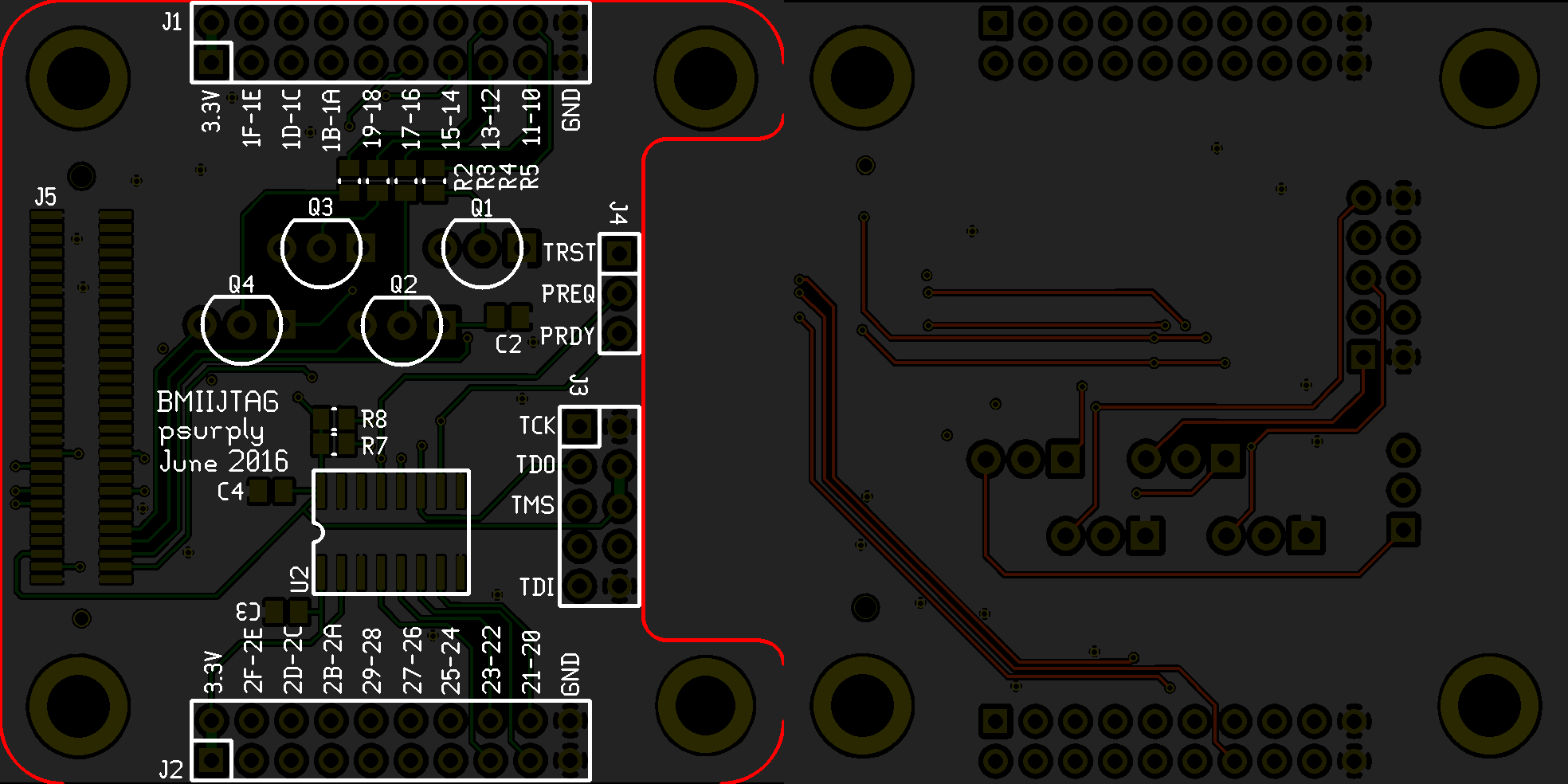
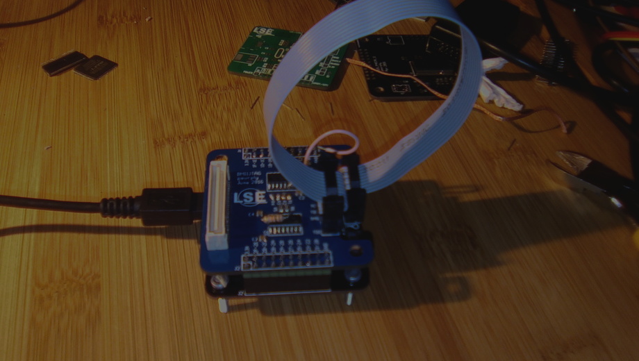
Section I: The Bridge Of Shockley
Even though the JTAG standard was quite strict about the communication logic, the electrical characteristics of the signals were left to the target device. This meant that the probe had the responsibility to drive them with the target voltage.
Assuming that the main board was only able to drive 3.3V IOs, expanding it with the needed interface was required.
A first version had been implemented using voltage level shifters and worked well with some mainstream devices. However, some platforms from specific manufacturers pull-up JTAG signals with very low resistors, which forced the probe to drive more current than most of the voltage level shifters could supply.
As a quick fix, the expansion board had been equipped with bipolar junction transistors for output signals.
In a more generic way, they though that being forced to design expansion board to electrically convert signals from the main board to the driven target was not a big deal. Main board’s IO could simply not be electrically universal.

Section II: The Self-Surgery
For a naive implementation of JTAG protocol, the IOModule consisted of simply
connecting the TMS and TDI outputs to a write-only control register while
wiring the TCK to its wr_pulse signal. In this configuration, each JTAG
clock tick was triggered by writing to this control register.
Each devices on a JTAG’s daisy chain communicated via a Test Access Port. This hardware unit implemented a stateful protocol to expose its debug facilities. As it was possible to make all of them converged to a reset and stable state, it was easy to walk though this state machine by keeping all TAPs synchronized.
Assuming this, a unique state machine was implemented in the IOModule to
keep the track of the current TAP state. A control register had been allocated
to allow the host to check this state when needed.
Devices responded to JTAG scans with the TDO signal. The FIFO block was
used to buffer received data before being read by the host thought a read-only
register. This case perfectly demonstrated the usage of the rd_pulse signal
since it was used to dequeue the next value of the FIFO submodule.

Although most platforms’s JTAG daisy chain were short and fixed, some of them could dynamically append TAP to the chain, making the usage of general purpose JTAG tools unusable. To describe this kind of situation, facilities had been implemented to describe a dynamic TAP network.
from bmii.modules.jtag import JTAG, TAP, DR
A JTAG object extended a regular BMIIModule to abstract the low-level
operations to the JTAG’s IOModule.
TAP and DR were provided to describe the current layout of the TAP network.
For instance, describing the Max V’s JTAG would look like this:
class AlteraMaxVJTAG(JTAG):
    def __init__(self):
        JTAG.__init__(self)

        tap = TAP("CPLDTAP", 10)    # 10-bit instrwuction register

        #          name             instr. reg.   length
        tap += DR("SAMPLE/PRELOAD", 0b0000000101, 480)
        tap += DR("EXTEST",         0b0000001111, 480)
        tap += DR("BYPASS",         0b1111111111, 1)
        tap += DR("USERCODE",       0b0000000111, 32)
        tap += DR("IDCODE",         0b0000000110, 32)
        tap += DR("HIGHZ",          0b0000001011, 1)
        tap += DR("CLAMP",          0b0000001010, 32)
        tap += DR("USER0",          0b0000001100, 32)
        tap += DR("USER1",          0b0000001110, 32)

        self.add_tap(tap)

        @classmethodw
        def default(cls, bmii):
            jtag = cls()
            bmii.add_module(jtag)

            bmii.ioctl.sb.pins.IO10 += jtag.iomodule.iosignals.TMS
            bmii.ioctl.sb.pins.IO11 += jtag.iomodule.iosignals.TCK
            bmii.ioctl.sb.pins.IO12 += jtag.iomodule.iosignals.TRST
            bmii.ioctl.sb.pins.IO13 += jtag.iomodule.iosignals.TDI
            bmii.ioctl.sb.pins.IO21 += jtag.iomodule.iosignals.TDO

            return jtag
According to that description, scanning the IDCODE of the device could be
simply done by:
b = BMII()
jtag = AlteraMaxVJTAG.default(b)

jtag.reset()
jtag.irdrscan("CPLDTAP", "IDCODE")
A possible improvement for this would be to generate this tap network directly from the BSDL files of daisy chained devices. The usage of BJT to drive JTAG signals was also a very quick and easy response to the low pull-up resistance problem. The third tinkerer complained that many other solutions could be implemented there as the BJT had a very long switching time and then forced to drive signals at 12MHz when many targets supported to be clocked up to 100MHz in their debug port.
Chapter IV: And In Darkness Bind Them
Sceptical about the results of the first application, the third tinkerer thought about a niche application that only few people would actually need. Enthusiastic but upset by the pragmatism of the two other, he left the group to develop his idea by his own.
For him, a second purpose for this board was purely and simply to act as a test bench for analysing black-boxed devices. To demonstrate his idea, he chose the first device he could found on his drawer: a Z80 packaged in a DIP-40.
Primary sold by Zilog as an improved Intel 8080, it had become a very popular processor for simple embedded applications since it was truly easy to make this chip working with a custom circuit. This device was then the perfect guinea pig for his experiences.
Section I: The Calm Before The Storm
Before trying to blow up the chip, defining the RTL needed to correctly drive the CPU was necessary.
iom = IOModule("Z80TB")
The DIP-40 version of this CPU exposed a 16-bit address bus and a 8-bit data
bus. As the last one was bidirectional, three different IOSignals had to be
defined: DIN, DOUT and DDIR. In order to keep the main board and the
device under test synchronized, the CPU’s clock was managed by the IOModule.
All other required control signals were defined as IOSignals.
ADDRESS_WIDTH = 14 # Truncated, actually 16.
DATA_WIDTH = 8

iom.iosignals += IOSignal("CLK", IOSignalDir.OUT)
iom.iosignals += IOSignal("_M1", IOSignalDir.IN)
iom.iosignals += IOSignal("_MREQ", IOSignalDir.IN)
iom.iosignals += IOSignal("_IOREQ", IOSignalDir.IN)
iom.iosignals += IOSignal("_RD", IOSignalDir.IN)
iom.iosignals += IOSignal("_WR", IOSignalDir.IN)
iom.iosignals += IOSignal("_WAIT", IOSignalDir.OUT)
iom.iosignals += IOSignal("_HALT", IOSignalDir.IN)
iom.iosignals += IOSignal("_RESET", IOSignalDir.OUT)
iom.iosignals += IOSignal("_RFSH", IOSignalDir.IN)

for i in range(ADDRESS_WIDTH):
    iom.iosignals += IOSignal("A{}".format(i), IOSignalDir.IN)

oe = Signal()
for i in range(DATA_WIDTH):
    iom.iosignals += IOSignal("DIN{}".format(i), IOSignalDir.IN)
    iom.iosignals += IOSignal("DOUT{}".format(i), IOSignalDir.OUT)
    iom.iosignals += IOSignal("DDIR{}".format(i), IOSignalDir.DIRCTL)
    iom.comb += getattr(iom.iosignals,"DDIR{}".format(i)).eq(oe)
From the host point of view, the only reasonable access points was the information about the state of the CPU, the address it was accessing and the data it transferred.
iom.cregs += CtrlReg("STATE", CtrlRegDir.RDONLY)

iom.cregs += CtrlReg("DIN", CtrlRegDir.RDONLY)
for i in range(DATA_WIDTH):
    iom.comb += iom.cregs.DIN[i].eq(getattr(iom.iosignals, "DIN{}".format(i)))

iom.cregs += CtrlReg("DOUT", CtrlRegDir.WRONLY)
for i in range(DATA_WIDTH):
    iom.comb += getattr(iom.iosignals, "DOUT{}".format(i)).eq(iom.cregs.DOUT[i])

iom.cregs += CtrlReg("ADDRL", CtrlRegDir.RDONLY)
iom.cregs += CtrlReg("ADDRH", CtrlRegDir.RDONLY)
for i in range(ADDRESS_WIDTH):
    if i < 8:
        addr = iom.cregs.ADDRL
    else:
        addr = iom.cregs.ADDRH
    iom.comb += addr[i % 8].eq(getattr(iom.iosignals, "A{}".format(i)))
A special control register had been added to perform special control
operations on the CPU. It was mainly used to manually control the RESET
signal forcing the reset of the chip from any CPU state.
iom.cregs += CtrlReg("CTL", CtrlRegDir.RDWR)
iom.cregs.CTL[0] = "RESET"

iom.comb += iom.iosignals._RESET.eq(~iom.cregs.CTL.RESET)
The clock signal of the Z80 had been fixed to half the frequency of the system clock. Due to clocking requirement of the chip, this signal was fixed to 8MHz.
iom.sync += iom.iosignals.CLK.eq(~iom.iosignals.CLK)
Requests from the Z80 CPU followed 3 stages. When it was not halted, the
testbench entered an IDLE state. During this one, the CPU was still
performing operations internally but did not request any external resources.
The second stage followed a request detection. The goal here was to freeze the CPU execution until the host provided an instruction to the testbench about how to handle the request.
Finally, the last stage meant actually responding to CPU’s request according to host instructions.

from enum import IntEnum

class Z80State(IntEnum):
    UNKNOWN = 0b00000000
    IDLE    = 0b00000001
    FETCH   = 0b00000010
    MEMRD   = 0b00000100
    MEMWR   = 0b00001000
    IORD    = 0b00010000
    IOWR    = 0b00100000
    HALTED  = 0b01000000
To implement this state machine in the RTL, Migen provided a facilities to define FSM in its generic library:
from migen.genlib

fsm = FSM()
iom.submodules += fsm

According to Z80 waveforms, the request for bus access was asserted using
_MREQ or _IOREQ. During the request initiation, _RD, _WR and address bus
are driven and valid.
When living the IDLE state, the testbench could determined what kind of
request was going to be performed and could notified the host about that.
fsm.act("IDLE",
    iom.cregs.STATE.eq(Z80State.IDLE),
    If(~iom.iosignals._HALT, NextState("HALTED")).\
    Else(
        If(~iom.iosignals._MREQ & iom.iosignals._RFSH,
            If(~iom.iosignals._RD,
                If(~iom.iosignals._M1, NextState("FETCH")).\
                Else(NextState("MEMRD"))).\
            Elif(~iom.iosignals._WR, NextState("MEMWR"))).\
        Elif(~iom.iosignals._IOREQ,
            If(~iom.iosignals._WR, NextState("IOWR")).\
            Elif(~iom.iosignals._RD, NextState("IORD")))))

fsm.act("HALTED",
    iom.cregs.STATE.eq(Z80State.HALTED),
    If(iom.iosignals._HALT, NextState("IDLE")))
While waiting for an answer from the host, the trick here was to assert the
_WAIT input of the CPU in order to notify it that bus cycle could not be
completed at that moment. This left enough time for the host to communicate its
desired operation. To finalize a write operation, the host just had to read
from the WRITE register. Completed a read operation was performed by
writing to READ control register.
bus_access = Signal()
iom.comb += iom.iosignals._WAIT.eq(~bus_access)

def goto_rd():
    return If(iom.cregs.DOUT.wr_pulse, NextState("READ"))

def goto_wr():
    return If(iom.cregs.DIN.rd_pulse, NextState("WRITE"))

fsm.act("FETCH",
    iom.cregs.STATE.eq(Z80State.FETCH),
    bus_access.eq(1),
    goto_rd())

fsm.act("MEMRD",
    iom.cregs.STATE.eq(Z80State.MEMRD),
    bus_access.eq(1),
    goto_rd())

fsm.act("MEMWR",
    iom.cregs.STATE.eq(Z80State.MEMWR),
    bus_access.eq(1),
    goto_wr())

fsm.act("IORD",
    iom.cregs.STATE.eq(Z80State.IORD),
    bus_access.eq(1),
    goto_rd())

fsm.act("IOWR",
    iom.cregs.STATE.eq(Z80State.IOWR),
    bus_access.eq(1),
    goto_wr())
To finally complete the bus cycle after intervention from the host, the data bus just had to be driven in the corresponding direction:
def goto_idle():
    return If(iom.iosignals._MREQ & iom.iosignals._IOREQ, NextState("IDLE"))

fsm.act("READ",
    iom.cregs.STATE.eq(Z80State.IDLE),
    oe.eq(1),
    goto_idle())

fsm.act("WRITE",
    iom.cregs.STATE.eq(Z80State.IDLE),
    goto_idle())
Section II: The Gates Open
Once the testbench logic defined, the BMIIModule could then be integrated to
a final BMII design:
z80tb = BMIIModule(iom)

b = BMII()
b.add_module(z80tb)
The actual wiring to the tested Z80 looked as follow. Due to the lake of physical IO pins on the main board, the two last pins of the address bus had been ignored.

The southbridge had to be informed to this configuration. Any changes on the
physical circuit only implied rerouting of the testbench’s IOModule on the
southbridge unit:
b.ioctl.sb.pins.IO28 += iom.iosignals._RESET
b.ioctl.sb.pins.IO29 += iom.iosignals._WAIT
b.ioctl.sb.pins.IO2A += iom.iosignals.CLK
b.ioctl.sb.pins.IO2B += iom.iosignals._M1
b.ioctl.sb.pins.IO2C += iom.iosignals._MREQ
b.ioctl.sb.pins.IO2D += iom.iosignals._IOREQ
b.ioctl.sb.pins.IO2E += iom.iosignals._RD
b.ioctl.sb.pins.IO2F += iom.iosignals._WR
b.ioctl.sb.pins.IO1F += iom.iosignals._HALT
b.ioctl.sb.pins.IO1E += iom.iosignals._RFSH

for i in range(ADDRESS_WIDTH):
    pin = getattr(b.ioctl.sb.pins, "IO1{}".format(hex(i)[2:].upper()))
    pin += getattr(iom.iosignals, "A{}".format(i))

for i in range(DATA_WIDTH):
    pin = getattr(b.ioctl.sb.pins, "IO2{}".format(i))
    pin += getattr(iom.iosignals, "DIN{}".format(i))
    pin += getattr(iom.iosignals, "DOUT{}".format(i))
    pin += getattr(iom.iosignals, "DDIR{}".format(i))
Section III: La Grande Illusion
As the IO controller design was completed, the host driver had to be completed in order to define the exact behaviour of the testbench.
For this example, the goal was to be able to execute a very short piece of code on the connected Z80. The content of the main memory had been defined as:
def ld_hl_nn(nn):
    return [0x2A, nn & 0xFF, (nn >> 8) & 0xFF]

def ld_b_n(n):
    return [0x06, n]

def ld_c_n(n):
    return [0x0E, n]

def otir():
    return [0xED, 0xB3]

def halt():
    return [0x76]


from itertools import chain, islice, repeat

s = "LSE"
instrs = chain(
    # Instructions
    ld_hl_nn(0x000A),    # 0000 - Load string address
    ld_b_n(len(s)),      # 0003 - Load string length
    ld_c_n(0),           # 0005 - Set IO port address
    otir(),              # 0007 - Output the string
    halt(),              # 0009 - Halt the CPU

    # Data
    [0x0C, 0x00],        # 000A - String address
    [ord(c) for c in s], # 000C - String content

    # Padding
    repeat(halt())       # Fill the rest of the memory
                         # with HALT instruction
)

mem = list(islice(instrs, 256))
The only job of the host was to poll the STATUS register and to reply by
reading from the DIN control register or by writing to DOUT according to
the CPU’s request.
recvbuff = ""

# Reset the CPU by pulsing the _RESET signal
z80tb.drv.CTL.RESET = 1
z80tb.drv.CTL.RESET = 0

while True:
    state = int(z80tb.drv.STATE)
    print("{}   \t-- Addr: {:04x}".format(str(Z80State(state)),
            (int(z80tb.drv.ADDRH) << 8) | int(z80tb.drv.ADDRL)),
         end='')

    # Emulate main memory reading
    if (state in [Z80State.FETCH, Z80State.MEMRD]):
        z80tb.drv.DOUT = mem[int(z80tb.drv.ADDRL)]

    # Emulate main memory writing
    elif (state == Z80State.MEMWR):
        mem[int(z80tb.drv.ADDRL)] = int(z80tb.drv.DIN)

    # Emulate reading from device
    elif (state == Z80State.IORD):
        z80tb.drv.DOUT = 0xFF

    # Emulate writing to device
    elif (state == Z80State.IOWR):
        data = int(z80tb.drv.DIN)
        recvbuff += chr(data)
        print(" | Data: {:02x} ({})".format(data, chr(data)), end='')

    # Stop main loop when CPU reaches the halt state
    elif (state == Z80State.HALTED):
        break
    print()

print("Received string: [{}]".format(recvbuff))

--
Z80State.FETCH   	-- Addr: 0000
Z80State.MEMRD   	-- Addr: 0001
Z80State.MEMRD   	-- Addr: 0002
Z80State.MEMRD   	-- Addr: 000a
Z80State.MEMRD   	-- Addr: 000b
Z80State.FETCH   	-- Addr: 0003
Z80State.MEMRD   	-- Addr: 0004
Z80State.FETCH   	-- Addr: 0005
Z80State.MEMRD   	-- Addr: 0006
Z80State.FETCH   	-- Addr: 0007
Z80State.FETCH   	-- Addr: 0008
Z80State.MEMRD   	-- Addr: 000c
Z80State.IOWR   	-- Addr: 0200 | Data: 4c (L)
Z80State.FETCH   	-- Addr: 0007
Z80State.FETCH   	-- Addr: 0008
Z80State.MEMRD   	-- Addr: 000d
Z80State.IOWR   	-- Addr: 0100 | Data: 53 (S)
Z80State.FETCH   	-- Addr: 0007
Z80State.FETCH   	-- Addr: 0008
Z80State.MEMRD   	-- Addr: 000e
Z80State.IOWR   	-- Addr: 0000 | Data: 45 (E)
Z80State.FETCH   	-- Addr: 0009
Z80State.HALTED   	-- Addr: 001f

Received string: [LSE]
Chapter V: The Feebleness Appears
In a meantime, the two other tinkerers were focussed on testing the main board on some more pragmatic scenarios in order to check its limitations with the hope to serve a real purpose.
Section I: The Relativity of Space…
Their experience with the implementation of a JTAG module were marked by the
difficulty to debug and trace the state of the digital design. As the
northbridge and the internal bus logic were considered reliable enough, they
decided to implement an IOModule exclusively designed to probe any other
signals of the IO controller design.
Acting as an internal logic analyser, a probing circuit composed of one control register fed by a FIFO was generated for each probed signals.
The capture was triggered by a special configurable signal and could be reset by the host at any moment.

As an example, the following design made the main board to act as a very cheap logic analyzer where all IO signals were simultaneously probed. The trigger was wired to the physical switch input:
b = BMII()
la = LogicAnalyzer(4) # Probing FIFO of 4 elements
b.add_module(la)

sb = b.modules.southbridge.iomodule

#        Probe name     Width   Signal
la.probe("IO1L",        8,      sb.cregs.PINSCAN1L)
la.probe("IO1H",        8,      sb.cregs.PINSCAN1H)
la.probe("IO2L",        8,      sb.cregs.PINSCAN2L)
la.probe("IO2H",        8,      sb.cregs.PINSCAN2H)
la.probe("IOMISC",      8,      sb.cregs.PINSCANMISC)

la.set_trigger(~sb.cregs.PINSCANMISC.SW)
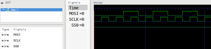
In parallel of that, an implementation of a master SPI module was in development. It was a perfect test case for the logic analyzer as it was not yet tested on a real SPI slave.
from bmii.modules.spi import SPIMaster
from bmii.modules.spidev import SerialFlash

b = BMII.default()
spi = SPIMaster.default(b)

la.probe("SCLK", 1, spi.iomodule.iosignals.SCLK)
la.probe("SS0", 1, spi.iomodule.iosignals.SS0)
la.probe("MOSI", 1, spi.iomodule.iosignals.MOSI)

la.set_trigger(spi.iomodule.cregs.TX.wr_pulse)
The SPI module initiated a transaction when its TX register was written. Its
wr_pulse was then used to define the trigger of the logic analyzer as the
goal was to analyse the output signal during an SPI activity.
The capture method of a logic analyzer object waited for a capture be
completed and then dequeued the samples by reading the control register of each
probe.
la.reset()
spi.select_slave(0)
spi.tranceive(42)

la.capture()
la.show()
Finally, the show method could be used to generate the captured waveforms to
a VCD file and to display it using gtkwave:
However, each probe circuit was significantly logicblock-consuming which limited the use of tiny FIFO making the logic analyser useless on complex circuit.
Section II: …And Time
After this first disappointment related to the quite limited space provided by the CPLD, they pursue their work on the SPI module by implementing required operations to drive a JEDEC-compliant serial flash memory.
sf = SerialFlash.default(b, spi, slave_id=0)
sf.read_id()
--
Manufacturer ID: 0xC2 (Macronix)
Memory Type: 0x20
Memory Capacity: 0x15 (16Mb)
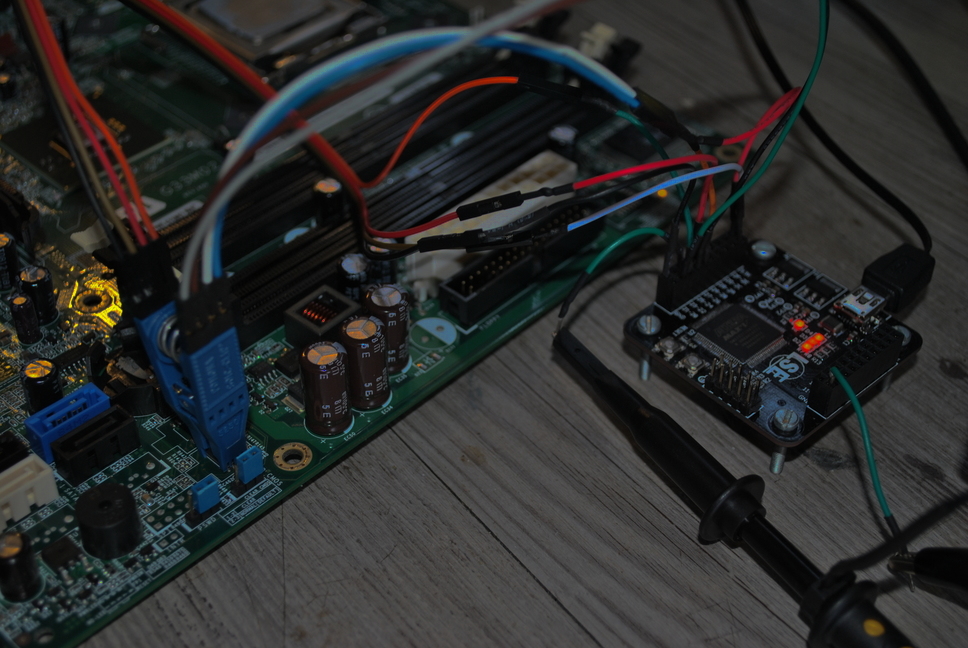
Driving the SPI flash was actually quite easy when it was previously extracted from its original circuit. This one was desoldered from a PC motherboard:
sf.dump(0x1FE000, size=25)

b'Award BootBlock BIOS v1.0'
The real challenge could be to probe the SPI packet in a passive way. This
implied to base the IOModule logic on the SPI clock imposed by an external
device instead of the regular system clock. Even though all this logic had been
implemented and tested on simple devices, it was still returning malformed data
when used on a PC motherboard since the BIOS flash was clocked at a frequency
higher than 40MHz.
Their guess for the reason of this issue was based on the fact that no IO pins were connected to a clock input of the CPLD. This meant that the SPI clock was gated by a regular IO input not designed to support such high frequency.
Chapter VI: Displayed As Of Yore
Affected by these previous failures, the two first tinkerers doubted about the real efficiency of the current hardware design of their board. By curiosity and driven by their discouragement, they look for the third one, probably lost in his solo projects.
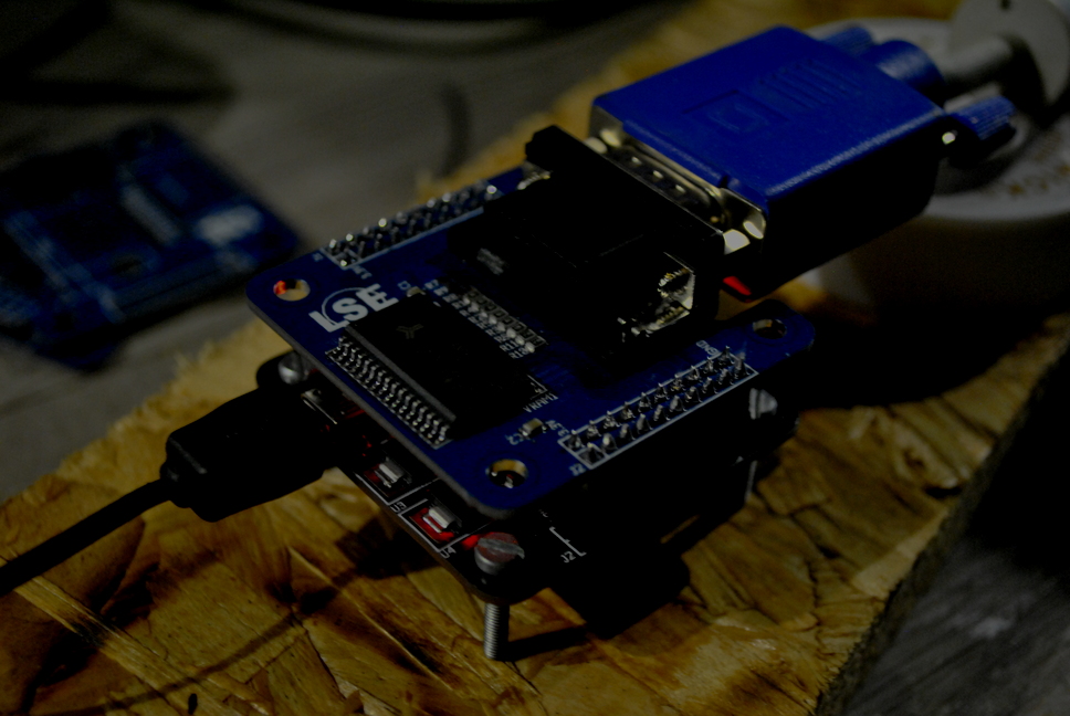
They found him in its basement, soldering wires and axial resistors to a VGA connector. He explained that he was oddly trying to make the main board acting as a video card. That was a plain useless job but he was glad to do it. Bored, the two other tried to helped him to finish and agreed that it would be their last experience with their board.
Section I: The Dilemma Of Etching Copper
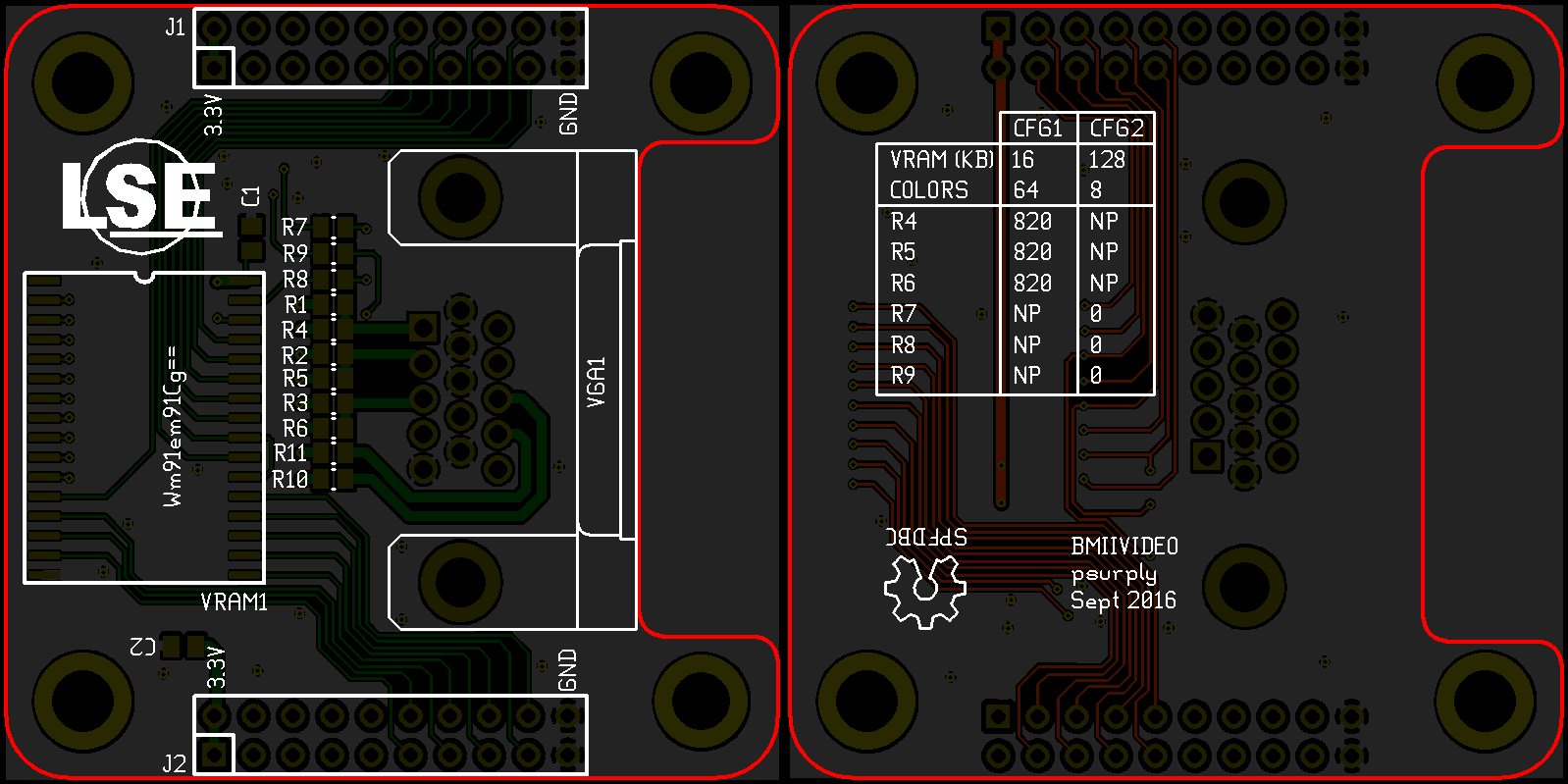
Although driving VGA signals was something quite simple, they estimated that creating a dedicated expansion board would make their job easier. Firstly, it would allow the mechanical integration of a decent VGA connector. Secondly, it was a good opportunity to add some extra memories to the board as the CPLD would not be able to store enough data needed to implement a video card. A standard 128KB static RAM packaged in a SSOP package has been chosen due to to its simple interface and its fast respond time.
The VGA’s RGB pins must be driven by analog signals which implied the use of
Digital to Analog Converters to be controlled from the CPLD. As these signals
were defined to be ground terminated by a 75 Ohm resistor on the monitor side,
a cheap equivalent of a DAC could be obtained by connecting different resistors
to several CPLD’s outputs, connected in parallel and acting as a voltage
divider with monitor’s termination resistor (see R1 to R6).
By allocating 6 outputs for driving RGB signals, 64 colors could be generated. However, the limited number of IO pins prevented the usage of all of the 17-pin SRAM’s address bus in the same time that the 6 pins of the RGB signals.
In order to postpone this design decision, jumpers had been added to the extension PCB to allow the configuration at soldering-time. The first setting allowed the usage of 8 colors with a 256KB video RAM while the second one constrained the use of a 16KB RAM but could drive 64 colors (see table at the bottom layer of the PCB).

Section II: A Proselytized Static Memory
On a regular video card, framebuffer was supposed to be stored on a dual-port RAM in order to allow the controller to write displayed frame in the same time that it was read by the signal generator. As this kind of device must be controlled by a large number of pin, a regular SRAM had been used to substitute a real VRAM.
Of course, this tweak forced a tighter management of the VRAM as two independents actors were using it at the same time while providing a unique interface.
From a high-level point of view the simple video card could be represented as an
IOModule by following this architecture:

To manage the VRAM, the trick was to exploit the fact that the pixel clock required to display with a resolution of 640x480 at 60Hz was fixed to 25.175 MHz. As the IO controller was clocked at 48MHz, odd ticks were used to read from VRAM and to drive the pixel clock at 24Mhz which was acceptable for most of the recent VGA monitors. Meanwhile, even ticks where used to perform the write operations on the VRAM. To ensure that writing operations were successful, the read operation that followed a writing was cancelled which was not critical most of the time but could led to small display glitches
The VRAM management unit could be described with the following state-machine:
- 1: If a write operation has to be performed, then, drive the data and the address bus. Else, drive the address bus for the next reading.
- 2: Reading state: Capture the output of the VRAM
- 3: Writing state: Indicate to the VRAM that the data bus is ready to be read for a memory writing.

Section III: Words Engraved In A Black Screen
As the VRAM management core logic and the VGA signal generation was correctly working, only the logic needed to drive the read from the VRAM and to drive RGB signals according to VRAM’s data had to be adapted to modify the displaying.
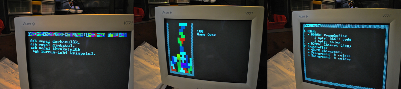
To demonstrate how the VRAM could be managed, a simple text mode had been implemented.
VRAM had been organized as follow:
0x0000- Text framebuffer: as the VGA-compatible text mode implemented on PC platforms, each characters consisted of one byte for the ASCII code and a second contained the color.0x0700- Character set (3KB): Sprites representing each character. A font similar to the IBM’s code page 437 was used.
As only one reading on the VRAM was possible per pixel clock tick, reading sequence had to be aligned to the character display. While the three last pixels of a character, the VRAM reading logic fetched the ASCII code and the color of the next character on the framebuffer and provided to the display logic the corresponding sprite’s row from the character set.

Epilogue
Surprisingly, the two first tinkerers found unexpected satisfaction to complete this dumb video card. The result of this last experience reflected the childish feelings that pushed them to start their first board: a satisfying design serving a useless objective.
This forced step-back helped them to highlight the items that could improve the next version of the board, if someone would be brave enough to go on on their footsteps. The lack of logic blocks could be easily solved by switching to an FPGA. A lot of decent ones were still available in 144-pin EQFP packages. Allocating pins to an external RAM would also not be a waste. Many other applications were blocked by the lack of an embedded and easy to use memory.
Concerning the timing issues encountered while probing the SPI flash, simply mapping some clock inputs to physical headers would be enough to unscramble most of them.
After that, the tinkerers team split up. Each of them had been aligned to the ‘state-of-art’-ish folk and they finally scattered, where engineers dwell…